Everyone has thought about building their own processor at some point, well, maybe not everyone, but I happen to be in that small group of people. Almost from the very beginning of my interest in electronics, I was most fascinated by its digital aspects, and although programming was much more impressive, I enjoyed designing logic circuits the most. In the past, I built various designs that could be called simple processors or microcontrollers, depending on the solutions used. These devices were based on basic logic circuits, and although they were impressive at the time, over time their expansion became increasingly difficult and expensive, especially for someone who had just started high school. Wanting to learn more about the secrets of digital technology, I had to go a step further, and that’s how I became interested in programmable circuits. This led to the creation of new designs based not on many separate chips, but on a single piece of silicon enclosed in an FPGA. However, I will talk about them, as well as the older, logical designs, in another article, because the subject of this text will be one of my most recent projects.
When searching the internet for the phrase “simple FPGA processor,” we find several interesting projects, mainly described in English, which, in my opinion, have one problem—none of these designs are simple. These projects are dedicated rather to enthusiasts and experts in FPGA circuits, and although from the perspective of a slightly more advanced user the project may not be too complicated, for beginners they will be black magic. In my opinion, many authors describing simple central processing units mistakenly assume that the reader is well versed in the intricacies of VHDL or Verilog and, in addition, is familiar with the principles of operation and design of this type of construction. This usually results in interesting projects, but ones that will be completely incomprehensible to a beginner.
Therefore, in this article, I would like to present one of my recent projects, a very simple soft processor implemented on an FPGA chip, which I have codenamed MS1. I will try to present it in the simplest way possible to avoid the effect I described above, which was my motivation for tackling this topic. The project is intended to be really simple, and before starting it, I set myself a few goals:
- The processor design (code) should be as simple as possible, preferably fitting into a single file.
- Based on Harvard architecture, where data and program memory are separated, which is a simpler concept to implement and understand.
- The number of commands supported has been reduced to a minimum, even at the expense of potential functionality. The project is primarily intended to describe a certain concept of how this type of structure works.
- The possibility of physical implementation on a real chip, not just operation in a simulator.
- The option of communicating with the outside world in the simplest form of parallel data input and output.
- The design is open and versatile enough to allow for potential expansion of the project without too much difficulty.
These are, of course, fairly general assumptions, but they define the MS1 project quite specifically. They can be summarized in three points: simplicity, versatility, and physical implementation.
In the following chapters, I will describe the general structure and characteristics of the processor, the commands it supports, and its operation, step by step. Then I will present its code in VHDL along with an explanation. In the last section, we will look at its operation both in a simulator and in a real environment.
Although the project is intended to be as accessible as possible to beginners, I will not focus on the absolute basics, because following that logic, I would have to start with a description of what electric current is, and that would significantly lengthen the entire topic. Of course, basic knowledge of what FPGA circuits are is useful, but for those unfamiliar with the subject, I will try to explain it in a few words. As I mentioned, I have built central units on single logic circuits in the past. As the complexity of the entire design increased, so did the number of chips used, which also increased the likelihood of potential problems. The FPGA chip was a wonderful panacea in this case. Composed of universal blocks, the chip allows you to build any logical structure on a single piece of silicon using hardware description language, without the need to involve many individual integrated circuits. This is a simple way to describe programmable chips – as universal integrated circuits whose operation depends on the user. However, they are not microcontrollers that execute a program stored in memory. FPGAs operate on code that is a description of the hardware – that is, a verbal description of logical structures that are further transformed into the internal configuration of the chip. In practice, this means that instead of writing successive instructions on “what to do,” as in the case of microcontroller programming, we describe “what is” the project implemented on the FPGA.
Architecture and construction of MS1
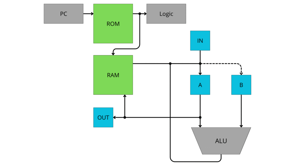
Like any processor, the MS1 design can be described using a block diagram. This is a graphical representation that makes it easier to understand how the system works as a whole, although it does not fully reflect the physical implementation of the CPU on the programmable chip. The processor consists of three types of functional blocks: registers marked in blue, memory modules marked in green, and other logic blocks marked in gray. It is an 8-bit unit, which means that the data is 8 bits long and the processor works with unsigned numbers ranging from zero to 255. The address buses are 4 bits wide, which allows for a maximum of 16 addresses to be addressed.
In accordance with the principles of Harvard architecture, memory is divided into two separate modules – ROM, which stores the program being executed, and RAM, which stores the data being processed by the CPU. Both blocks have the same capacity of 128B, in a 16x8b configuration. The program memory is addressed from the PC (program counter), a special counter that increases its value after each instruction is executed. The 8-bit ROM data output is divided into two parts – operand and opcode, each of which has 4 bits. The operand is a signal transmitted to the RAM memory, acting as an address, which allows you to refer to the data stored in it. The opcode, which is the code of the command to be executed by the processor, is sent to the Logic block, where all the magic happens. The instruction is decoded there and used to control other processor blocks in order to execute the appropriate instruction.
MS1 is based on only four registers. IN and OUT are used for communication with the outside world, with eight physical outputs of the FPGA connected to each of them. This makes it possible to read data via the IN register and control, for example, eight LEDs connected to OUT, which will represent the data processed by the CPU. The main register of MS1 is A, which can store information from RAM, the IN register, or the ALU unit. The line leading to register B has been deliberately marked with a dotted line because its input is connected only to the RAM data output, and only RAM can be the source of information for this register.
Registers A and B form a pair that stores numbers on which arithmetic operations are performed. These are addition and subtraction, physically performed in the ALU, or arithmetic logic unit. As you can see, MS1 only executes arithmetic commands, and the name AU, arithmetic unit, would be more appropriate here, but I decided not to introduce unnecessary confusion in the nomenclature, because it is common practice to refer to such blocks as ALUs, even if they are very simple.
MS1 Instructions
Opcode | Operand | Instruction | Description |
0000 | XXXX | NOP | Don’t do anything |
0001 | ADDR | LD A | Enter the value from the address into register A |
0010 | ADDR | LD B | Enter the value from the address into register B |
0011 | ADDR | STR A | Enter the value from register A into memory |
0100 | XXXX | ADD | Addition (A+B) result in A |
0101 | XXXX | SUB | Subtraction (A-B) result in A |
1000 | XXXX | OUT | Enter the value from A into the OUT register |
1001 | XXXX | IN | Enter the value from IN into register A |
1111 | XXXX | HLT | Stop the CPU |
The MS1 processor supports nine commands, which can be grouped into three categories: transfers, operations, and special commands. Each instruction consists of eight bits, four opcodes, and four operands, stored in ROM. The opcode is a unique value assigned to a specific command, while the operand acts as a four-bit address for commands that require this parameter. In the table, these are the places described as ADDR, but in most cases the value stored in this place is irrelevant to the instruction being executed; these are the places described as XXXX.
MS1 supports five data transfer commands. LD A and LD B write data from RAM to the appropriate registers, with the specific memory address determined by the operand. The STR A instruction has the opposite effect and writes data from register A to RAM at the address specified by the operand. OUT and IN are instructions that allow the central processing unit to communicate with the outside world. They allow data to be written to the OUT register, whose output is connected to the outside, or to the IN register, whose input is connected to external outputs. Both commands also refer to register A, from which or to which data is written.
The arithmetic instructions supported by the CPU are addition and subtraction. They refer to the values stored in registers A and B, where the value in the former is always more significant. This means that a value is added to or subtracted from it. After the operation is performed, the result is written to register A.
The processor also supports two special commands, NOP and HLT. The first one is an empty instruction that is executed but does not cause any changes. The second instruction, HLT, is a command that stops the processor when it encounters the value 1111 in ROM, and it stops fetching further instructions from memory. It is only possible to exit this state by means of an external reset or by disconnecting the power supply.
How does MS1 work?
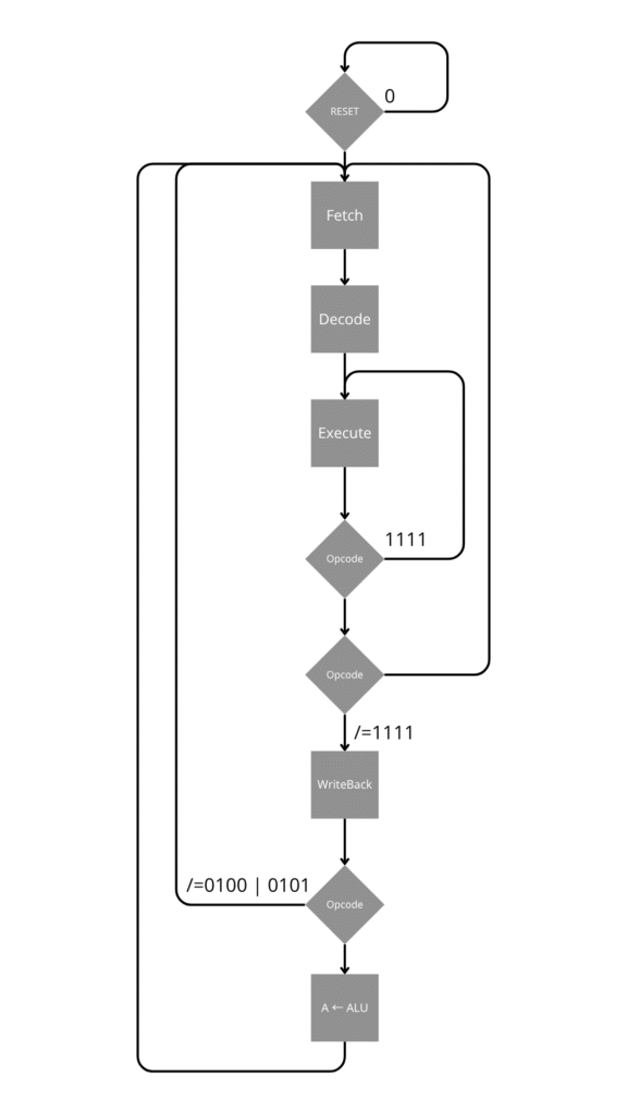
Let us now move on to the general principle of operation of the MS1 processor, which will make it easier to describe the code that we will deal with in the next chapter. Basically, we could describe its operation using four states – Fetch, Decode, Execute, and WriteBack. They occur one after another, and in each one the processor performs specific functions to execute the given command. However, although this description is true, it does not cover the subject in any detail. That is why I have prepared a short algorithm that describes the operation of MS1 in a little more detail.
In the first step after startup, the chip checks the status of the reset signal. As I mentioned when analyzing the command list, this is external, which means that a button performing this function is connected to one of the FPGA chip outputs. If the reset signal is in the zero state (it operates in negative logic), the processor will not execute the program stored in memory, and all its internal registers will be restored to their default state. Only when the reset enters the one state, for example after releasing the button, will the processor start operating. At this point, another condition, which we can call the master condition, will be checked. MS1, like similar designs, is a synchronous project. This means that it needs an appropriate clock signal to operate, which determines the subsequent steps in its functioning. The clock signal, like the reset, is external and comes from a quartz generator. It was intentional not to mention the MS1 clock frequency earlier, because it can be arbitrary, depending on the hardware platform on which the design will be run; in my case, it is 50MHz. If the reset is not active, the CPU waits for the rising edge of the clock and when it appears, it performs a single step. In this way, we can describe the general operation of MS1, determining whether it executes the program or is looped in the reset function.
Let us now move on to the issue of program execution and the aforementioned processor states. The first one that the CPU will execute is Fetch. This is the first step in which an instruction is retrieved from the ROM. The location from which it will be retrieved is defined by the value of the program counter PC. After the first start, it will be address zero.
Once the command has been fetched, we move on to decoding it – Decode. In this step, it is divided into Opcode and Operand, which are quite important from the perspective of what the processor is supposed to do. I described their meaning when presenting the list of commands.
After preparing the Opcode and Operand values, MS1 proceeds to execute the command – Execute. What exactly happens is defined by the aforementioned values. We will take a closer look at this later when analyzing the code, but at this point it is worth mentioning that most commands involve sending data or calling an arithmetic function. The exception here is the HLT instruction, which is highlighted in the MS1 operation network. The processor checks whether the Opcode has a value of 1111, and if so, the Execute step is performed again. In other words, the processor will enter an infinite loop, which from the user’s perspective will look like it has stopped working. The only way to exit this state is to activate a reset or disconnect the power supply. It is worth mentioning that after the command is executed, the PC command counter is incremented, which is a preparation for executing the next instruction stored in the ROM.
If the CPU executes a command other than HLT, we can proceed to the next Opcode check. If its value is other than 1111, we call the WriteBack state. Otherwise, we return to the Fetch state, which should never happen because the processor should enter an infinite loop earlier. This functionality is only an additional security measure.
In the WriteBack state, the processor checks whether a command related to the arithmetic logic unit (ALU) has been executed. If this is true, the result from the output of this module is written to register A, where all arithmetic operation results are stored. Regardless of whether this process is completed, this is the moment when MS1 finishes executing a single instruction. We then return to the Fetch state, where the next command will be fetched from the program counter address, which has been incremented by one during the Execute state.
This is a brief description of how MS1 works, which will certainly become clearer upon closer examination of the equipment description.
Processor code
As intended, the hardware description of the MS1 processor is quite short and fits into a single file. The whole thing takes up about 100 lines of VHDL code, approximately, because this number may be slightly higher if the processor is running a more complex program stored in ROM. In fact, the description could be even shorter than 100 lines, but this would make it less readable. You can find the code as a whole on my GitHub profile. I encourage you to take a look at it, as it will give you a broader perspective.
library IEEE;
use IEEE.STD_LOGIC_1164.ALL;
use IEEE.NUMERIC_STD.ALL;
The project begins in a fairly standard manner, typical for FPGA-based designs. Here, we have three lines importing the libraries necessary for working with logic signals and numeric types.
entity cpu is
    Port (
        clk     : in  STD_LOGIC;
        rst     : in  STD_LOGIC;
        input_port : in  STD_LOGIC_VECTOR(7 downto 0);
        output_port : out STD_LOGIC_VECTOR(7 downto 0)
    );
end cpu;
Next, there is a description of the ports available on the MS1. These are: clock signal input – clk, reset signal input – rst, data input port – input_port, and data output port – output_port. It is worth noting that both ports are 8-bit.
architecture Behavioral of cpu is

    type state_type is (Fetch, Decode, Execute, WriteBack);
    signal state : state_type := Fetch;

    signal pc        : unsigned(3 downto 0) := (others => '0');
    signal instr     : STD_LOGIC_VECTOR(7 downto 0);
    signal opcode    : STD_LOGIC_VECTOR(3 downto 0);
    signal operand   : STD_LOGIC_VECTOR(3 downto 0);

    signal regA      : STD_LOGIC_VECTOR(7 downto 0) := (others => '0');
    signal regB      : STD_LOGIC_VECTOR(7 downto 0) := (others => '0');
    signal alu_result: STD_LOGIC_VECTOR(7 downto 0);
In the first part of the architecture block, we create an enumeration type state_type, which can take one of four states – Fetch, Decode, Execute, and WriteBack. Next, we declare a signal state, whose type is state_type. In other words, this describes a state machine that determines what the processor will do at a given moment. The state value will change during the operation of MS1, but by default, the current state after startup will be Fetch, as defined by the notation “:=Fetch;”.
Next, registers and auxiliary signals were declared. The pc signal acts as a command counter; it is a four-bit unsigned signal whose base value after processor startup is zero.
The instr, opcode, and operand vectors are associated with ROM memory. The first of these will store the value retrieved from memory, which will then be assigned to the opcode and operand signals in the next step. As you can see, instr is 8 bits long, which are then divided into two equal parts.
Next, registers A and B were placed, the significance of which I mentioned when describing the architecture. Their default value is zero. Alu_result is a signal associated with the arithmetic logic unit. It will store the result generated by the ALU when it has not yet been written to register A.
    type memory_type is array (0 to 15) of STD_LOGIC_VECTOR(7 downto 0);
    signal ROM : memory_type := (
        0 => "00010000", -- LD A, 0
        1 => "00100001", -- LD B, 1
        2 => "01000000", -- ADD
        3 => "00100010", -- LD B, 2
        4 => "01000000", -- ADD
        5 => "10000000", -- OUT
        6 => "11110000", --HLT
        others => (others => '0')
    );
    signal RAM : memory_type := (
        0 => "00000010", -- 2
        1 => "00000001", -- 1
        2 => "00000001", -- 1
        others => (others => '0'));
ROM and RAM memory have been defined as sixteen-element memeory_type arrays, in which 8-bit logical vectors are stored. Both modules have been filled with sample data. In the ROM memory, I placed a simple program that adds two numbers stored in RAM and then adds another number to the result. After these operations, the result is sent to the OUT port and the processor is stopped. This example clearly shows the structure of data that are commands, with the four most significant bits being the opcode specifying the function to be performed by MS1. The next bits can be the address for RAM, as is the case with LD commands. The first one refers to address zero in RAM, where the number two is stored, the second to address one, where the number one is stored, and the third LD command uses the second cell, where the number one is also stored.
    process(clk, rst)
    begin
        if rst = '0' then
            pc <= (others => '0');
            instr <= (others => '0');
            opcode <= (others => '0');
            operand <= (others => '0');
            regA <= (others => '0');
            regB <= (others => '0');
            alu_result <= (others => '0');
            output_port <= (others => '0');
            state <= Fetch;
The CPU’s operation is described by a synchronous block process dependent on the clk and rst signals, which are key or superior here, as I mentioned earlier. The first condition that MS1 checks is the status of the reset signal. When it is active, i.e., its value is zero, all signals and registers are reset, and the state machine assumes the Fetch value.
        elsif rising_edge(clk) then
            case state is
                when Fetch =>
                    instr <= ROM(to_integer(pc));
                    state <= Decode;
                when Decode =>
                    opcode <= instr(7 downto 4);
                    operand <= instr(3 downto 0);
                    state <= Execute;
If the rst signal is not active, the processor checks whether there is a rising edge of the clock signal, which defines the subsequent CPU cycles. When this occurs, we proceed to execute the command. The whole process is based on the case function dependent on state, i.e. the state machine. Depending on the value, a different piece of code will be executed. If the Fetch state is currently active, the processor will assign the value stored in the ROM, from the address specified by pc, to the instr signal and simultaneously assign a new state to the state machine – Decode, so that on the next CPU clock cycle it will convert instr to opcode and operand. This also happens in the next fragment of code with the next state change, which is assigned the value Execute.
                when Execute =>
                    case opcode is
                        when "0000" => -- NOP
                            null;
                        when "0001" => -- LD A
                            regA <= RAM(to_integer(unsigned(operand)));
                        when "0010" => -- LD B
                            regB <= RAM(to_integer(unsigned(operand)));
                        when "0011" => -- STR A
                            RAM(to_integer(unsigned(operand))) <= regA;
                        when "0100" => -- ADD
                            alu_result <= std_logic_vector(unsigned(regA) + unsigned(regB));
                        when "0101" => -- SUB
                            alu_result <= std_logic_vector(unsigned(regA) - unsigned(regB));
                        when "1000" => -- OUT
                            output_port <= regA;
                        when "1001" => -- IN
                            regA <= input_port;
                        when "1111" => -- HLT
                            state <= Execute;
                        when others =>
                            null;
                    end case;
                    if opcode /= "1111" then
                        state <= WriteBack;
                    end if;
The fragment of code responsible for executing the command is definitely the most active. There is another case function here, depending on the opcode value. As you can see, all commands are described in a similar way, so we will analyze them one by one.
The NOP instruction does not change anything, hence the “null;” entry. Loading data into registers A and B works on the same principle, i.e., assigning to regA and regB a signal from RAM specified by the address stored by the operand signal. Writing data to RAM is also similar, except that this time the value from regA is assigned to the RAM signal specified by the operand. Next are the arithmetic functions that assign the results of addition or subtraction to alu_result. The OUT and IN commands are nothing more than transferring data from regA to output_port or from input_port to regA.
The last supported function is HLT, which, as I mentioned earlier, causes the processor to loop. It reactivates the Execute state, so that on the next clock cycle, it will be executed immediately and will encounter the HLT command again, because the states of the signals and registers will not be modified. In this way, MS1 will enter an infinite loop, continuously executing the HLT command. It is also worth mentioning the “when others =>” notation. As you can see, when a value that does not correspond to any of the commands is found in memory, the processor will treat it as an empty NOP instruction.
In addition to the case function, there is also a small condition that checks whether the previously executed command was different from “1111”, in other words, whether it was a command other than HLT. If so, the state machine will take the value WriteBack, allowing the processor to move on to the next step.
                when WriteBack =>
                    if opcode = "0100" or opcode = "0101" then
                        regA <= alu_result;
                    end if;
                    pc <= pc + 1;
                    state <= Fetch;
            end case;
        end if;
    end process;

end Behavioral;
WriteBack is the last state of the processor. When it is executed, the opcode is checked, more specifically whether its value was “0100” or “0101”, which means that one of the arithmetic commands was executed. If this is true, the value from the alu_result signal is assigned to register A so that when the next instruction is executed, the result is placed in that location.
In addition, the last state of the processor also increases the pc command counter by one, so that the next command in the queue will be fetched during the next cycle. Additionally, the state machine is set to Fetch and the entire procedure is performed again.
MS1 implementation
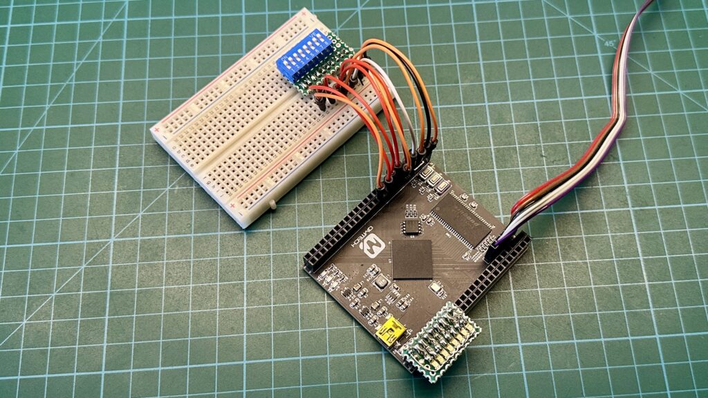
One of the objectives of the MS1 project was its physical implementation. For this purpose, I used one of my boards, specifically a small design manufactured by Qmtech. The module is equipped with an Xilinx FPGA chip from the Artix-7 family – XC7A35T. The board also features an SDRAM memory chip (unused), three buttons, one of which I adapted to serve as a reset button, three LEDs, and a 50MHz quartz signal generator, which serves as the processor’s clk signal. In addition, I connected eight LEDs (output_port) and an eight-position DipSwitch (input_port) to the external pins.
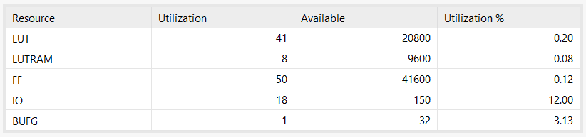
I prepared the design in Vivado, and you can find its compressed form on my GitHub profile. MS1 is not a very demanding design and can be implemented on virtually any FPGA chip. It requires 41 basic LUT logic blocks, 8 LUTRAM blocks for memory implementation, 50 FF registers, 18 I/O pins, and one clock buffer.
Analysis of a sample program
Let us now analyze an example program that MS1 can execute. We will use input/output ports, RAM, and the addition function. Below is a code snippet with properly configured ROM and RAM.
    signal ROM : memory_type := (
        0 => "10010000", -- IN
        1 => "00100001", -- LD B, ADDR:1
        2 => "01000000", -- ADD
        3 => "10000000", -- OUT
        4 => "11110000", -- HLT
        others => (others => '0')
    );
    signal RAM : memory_type := (
        0 => "00000000", -- 0
        1 => "00011010", -- 26
        2 => "00000000", -- 0
        others => (others => '0'));
As you can see, the program consists of five commands. First, we read the value from the input port and store it in register A. The next step is to retrieve the value stored at the first address from RAM and place it in register B. We add the prepared data, and the result is sent to register A, from where it is copied and transferred to the output port. After these operations, the processor is stopped with the HLT command.
The number 26 has been stored in RAM at the first address, and the program will add any value taken from the IN register to it.
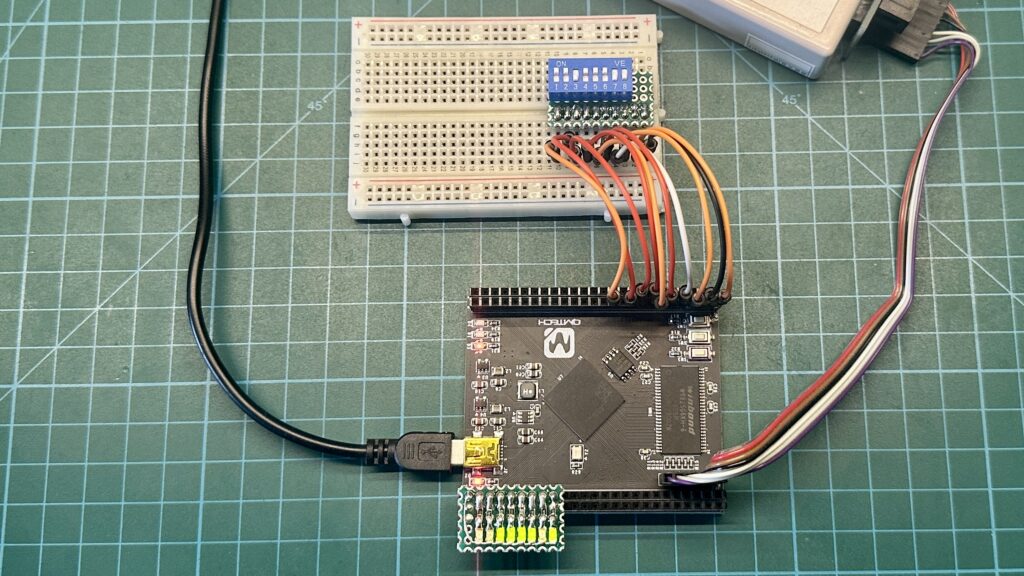
In the attached image, you can see how the program works in practice. Using the DipSwitch switch, I set the value to 35 (00100011), which is then retrieved by the processor. After adding the number 26 from memory, we obtain 61, which is transferred to the output port, allowing us to see the binary representation of this value, i.e. 00111101.
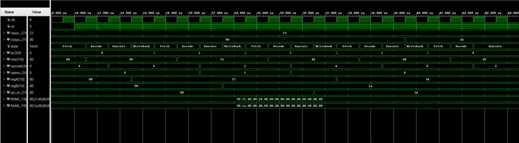
In addition to the actual launch, I also ran a simulation of the program, which illustrates quite well what happens to the processor with each successive clock cycle. Importantly, all values visible in the simulation are in hexadecimal form. The CPU starts operating when the reset signal value changes to one. Then the first instruction 0x90 is fetched, it is divided into an opcode and an operand, and the result of its operation is the appearance of the value from the input, i.e. 0x23 (35), in register A. Then the next instruction is handled, as you can see, the operand changes its value to the address that is passed to RAM. After its execution, 0x1A, or 26, appears in register B. In the next step, the values are added, which can also be seen in the sequence, because the result of this operation appears in register A – 0x3D (61). This value still needs to be transferred to the output register, which happens in the last step. At the very end, you can also see the processor entering a permanent Execute state, i.e., the execution of the HLT command.
What's next?
The capabilities of the MS1 processor are quite small, this is the cost of its very simple construction, but this was the intention of this design. It is intended to introduce the concept of CPU implementation to all those who may be just beginning their adventure with FPGAs. Also, for those more advanced users, it can be a good foundation for creating their own more elaborate design.
Personally, I intend to continue this project to show just the process of its expansion. The first thing to do, of course, is to expand the memory, expand the capabilities of the ALU, add conditional and unconditional jump instructions and software control of the clock frequency, along with the possibility of stepping, which will greatly improve the debugging process. A processor with such capabilities will already be much more “usable”, because MS1, after all, is more of a showpiece than a useful thing.
Finally, I encourage your own experiments, opinions and ideas that you can share.