This article is an archival post from my first website created around 2017. The quality of the graphics is not the best, as I unfortunately no longer have access to the originals, but for the sake of preserving the memory of this project, I am providing related materials.
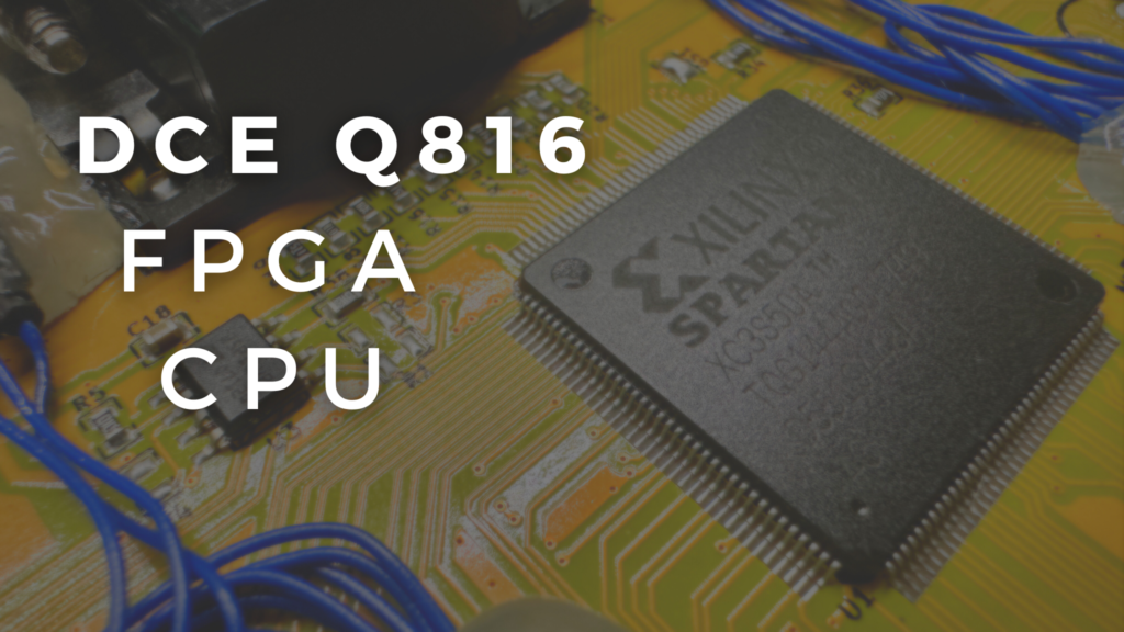
The DCE system is a processor (DCE Q816) and coprocessor (DCE Q817) designed by me and run on FPGAs. It was created while I was learning the VHDL language and learning about FPGA circuits in general. I decided to share my project with others to make them curious about FPGAs.
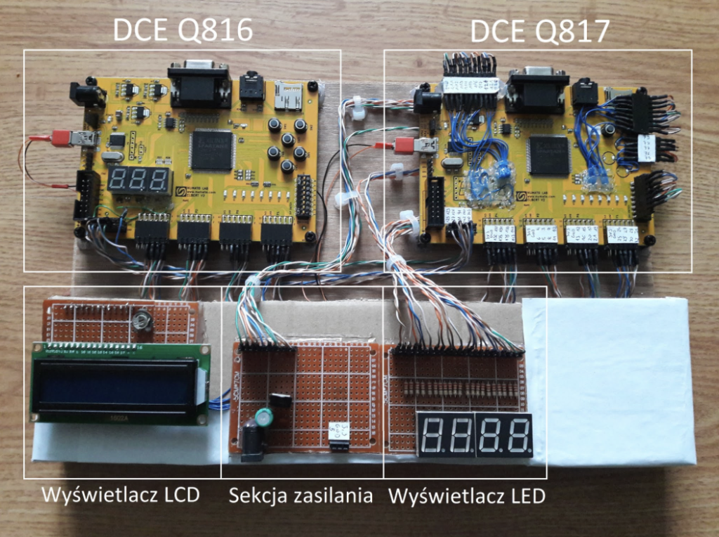
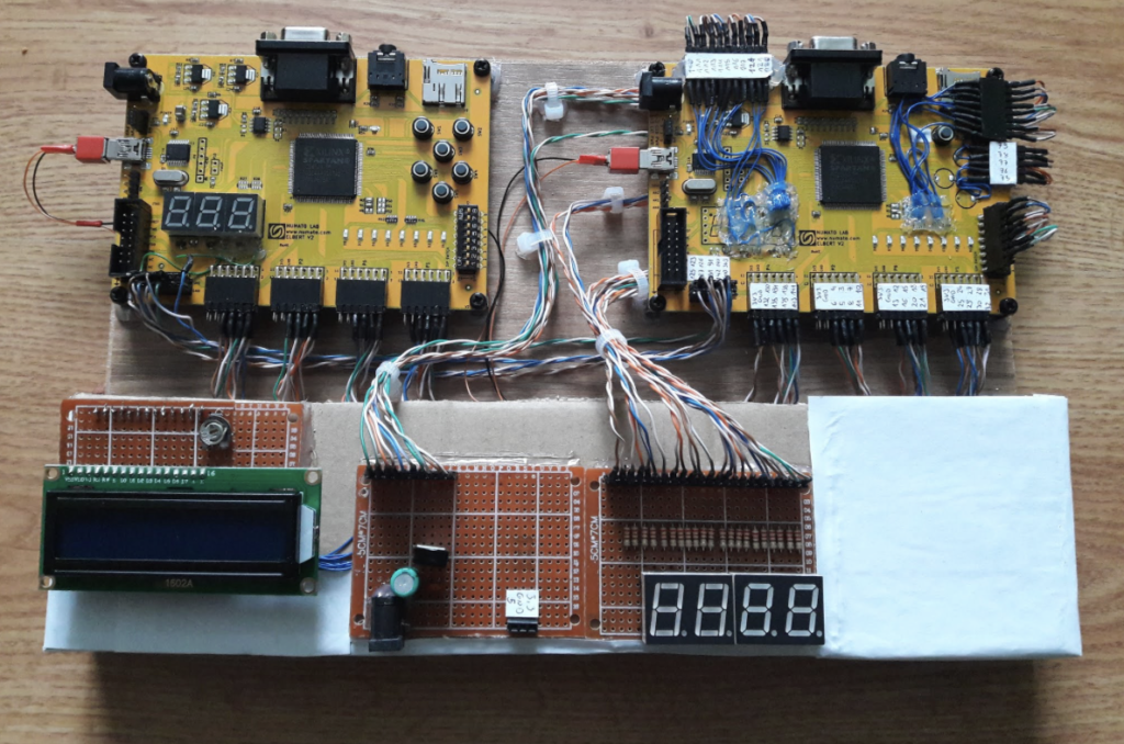
The project was implemented on two Elbert v2 boards, equipped with Xilinx Spartan XC3S50A chips. As you can see, one as well as the other board has undergone appropriate modifications. On the DCE Q816 processor board, the 7-segment displays were disconnected. The DCE Q817 coprocessor board has undergone much more. Here, the 7-segment displays and five buttons were completely removed and the LEDs and Dipswitches were disconnected. Modifications were made to increase the number of available pins.
Below the FPGA circuit boards, we see three more components of the DCE system. These are an LCD display based on the HD44780 controller, a power section that supplies the appropriate voltage to the other circuits, and four 7-segment displays, of which three are active.
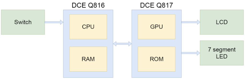
Above we can see a general schematic of the DCE system. The main component is the DCE Q816 processor, which contains the central processing unit (CPU) and RAM. Eight Dipswitches are connected to its input. Another component is the DCE Q817 coprocessor. It performs the function of the ROM, where the executed program is stored, and the graphics processor. It takes care of generating signals for LCD and LED displays connected to the coprocessor’s outputs.
DCE Q816 is an 8-bit processor realized on an FPGA chip. It works in conjunction with the DCE Q817 coprocessor. The chip was based on the MS2 architecture. It is my own concept based on the Harvard architecture (program and operational memory are physically separated). The processor is clocked with a 12MHz signal, but the chip supports software frequency change. We have the possibility to reduce this value even to 2.8Hz. The processor has an 8-bit input connector and a 16-bit output connector. In addition, the chip has an input for an external RESET signal.
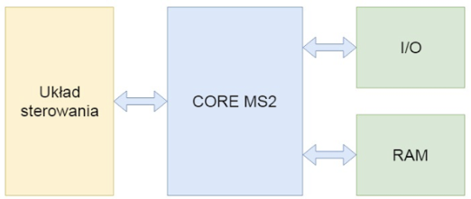
Above we see that the CPU is based on four functional blocks. The CORE MS2 execution core is where all arithmetic and logic operations are performed. Control circuit this is where all control signals are generated. RAM (operational memory) with a capacity of 2kb (256B) realized on the memory block inside the FPGA chip. The last component is the I/O (input/output) block, which supports input/output ports.
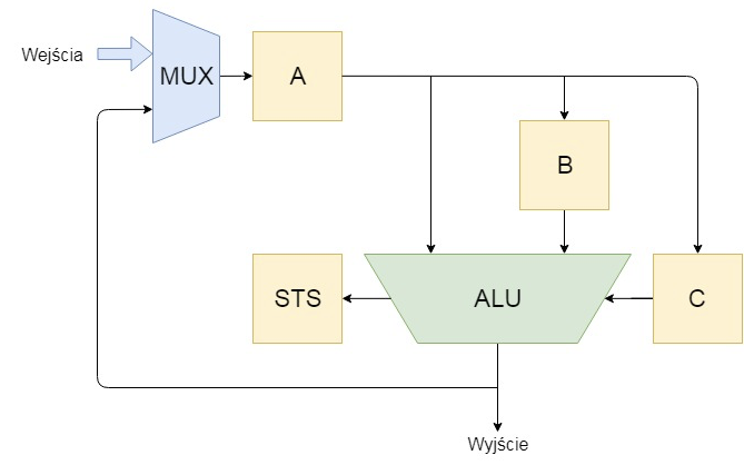
The CORE MS2 logic (execution) core is the main component of the DCE Q816 processor. It is here that all arithmetic and logic operations are performed. It includes an arithmetic logic unit (ALU), an input multiplexer and a set of registers.
Register A is the first memory element, it is here that all data is stored regardless of further destination. Register B stores the second variable for the ALU. Register C stores the command for the ALU. The last register is STS. This is a 4-bit register that stores information about the so-called status bits. These are needed to execute conditional jump commands.
|
Carry bit |
State bit |
||
|
Cout |
A=B |
A>B |
A<B |
In the table we see the exact structure of the STS register. The first three bits (from the right) determine the relationship between the variable stored in the A register and B. Simply put, if the variable stored in B is greater than the one stored in A then the first bit (A<B) will take the value of one. The last bit of the STS register is Cout the so-called transfer bit. It informs that the result of the operation carried out by the arithmetic-logic unit (ALU) exceeded the range of 8 bits. The output of the STS register is connected to the control system.
The MUX, or input multiplexer, is the element that selects which input signal to write to the A register. This signal is selected based on the command being executed.
The main component of the CORE MS2’s execution core is the arithmetic logic unit (ALU). It is here that operations are performed on variables stored in registers A and B, according to the command stored in register C. In Table 2 we see all the commands supported by the ALU.
|
Binary code |
Command |
Description |
|
0000 |
A |
Send A |
|
0001 |
A+1 |
Incrementation A |
|
0010 |
A+B |
Add |
|
0011 |
A-B |
Sub |
|
0100 |
A and B |
Logic operation |
|
0101 |
A or B |
|
|
0110 |
A xor B |
|
|
0111 |
A nand B |
|
|
1000 |
A nor B |
|
|
1001 |
A xnor B |
|
|
1010 |
not A |
|
|
1011 |
PL |
Shift left |
|
1100 |
PR |
Shift right |
|
1101 |
RL |
Rotate left |
|
1110 |
RP |
Rotate right |
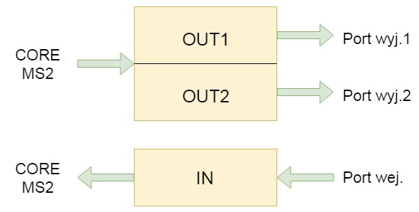
The I/O circuit is actually a set of three registers IN, OUT1, OUT2. As you can guess one of them is input the other two are output. The processor stores in them all the data it receives from outside and those it wants to send outside. It can be said that they act as communicators with the outside world.
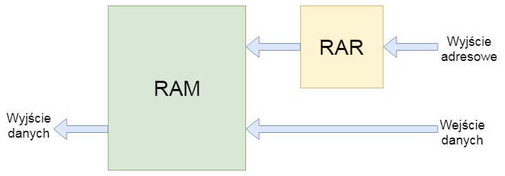
The RAM block consists of two elements of the RAR register storing the address and the memory itself. The block available inside the FPGA chip was used to implement the memory. The memory cell addresses are 8 bits wide giving a total capacity of 2k bits (256 bytes).
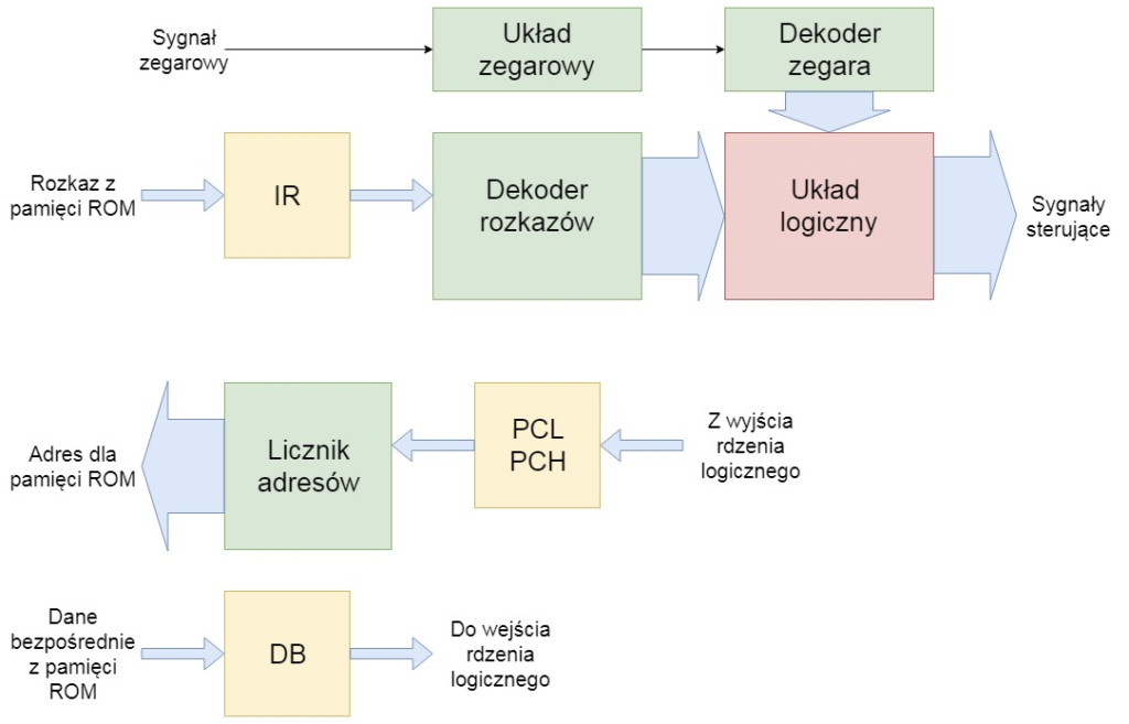
The control circuit is the most advanced part of the processor. It is here that all control signals are generated based on the command and the clock signal. In addition, the control circuit includes: an address counter for the ROM along with registers storing addresses for jumps, a DB register storing a variable directly received from the ROM.
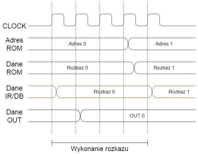
In the image we see simplified timing waveforms for the DCE Q816 processor. We can see that it takes four clock bars to execute a single command regardless of its type. Four signals are described in the figure. The first one is ROM Address, which is the address for the program memory. As you can see, the value of the address changes at the fourth clock bar, it can be an increase by one or a jump to the address stored in the PCL and PCH registers. The next signal is a variable appearing at the input of the processor. The variable appears there just after the address change. IR/DB data is the determination of the outputs of the IR (instruction register) and DB (direct data) registers. It is on the basis of the data stored in these registers that the command that the processor executes is determined. Writing to these registers is done on the first clock beat. The last signal determines what is at the output of the chip. Updating the contents of the OUT registers and most of the processor’s registers takes place on the second clock beat.
This is a rather simplified diagram of how the processor works, but it can be put even more simply. The chip takes instructions from ROM. It executes it. It increments or sets the address to fetch the next instruction and everything executes again.
Lp. | Kod binarny | Nazwa | Opis |
1 | 00000 | NOP | Nie rób nic |
2 | 00001 | AC | Prześlij zmienną z wyjścia CORE MS2 do A |
3 | 00010 | AIN | Prześlij zawartość z rejestru IN do A |
4 | 00011 | ADB | Prześlij zawartość z rejestru DB do A |
5 | 00100 | ARAM | Prześlij zawartość z pamięci RAM do A |
6 | 00101 | B | Prześlij zawartość z rejestru A do B |
7 | 00110 | C | Prześlij zawartość z rejestru A do C |
8 | 00111 | RAMA | Zapisz do rejestru adresowego pamięci RAM wartość z wyjścia CORE MS2 |
9 | 01000 | RAMD | Zapisz do pamięci RAM wartość z wyjścia CORE MS2 |
10 | 01001 | OUT1 | Zapisz do rejestru OUT1 wartość z wyjścia CORE MS2 |
11 | 01010 | OUT2 | Zapisz do rejestru OUT2 wartość z wyjścia CORE MS2 |
12 | 01011 | PCL | Zapisz do rejestru PCL wartość z wyjścia CORE MS2 |
13 | 01100 | PCH | Zapisz do rejestru PCH wartość z wyjścia CORE MS2 |
14 | 01101 | IN | Zapisz wartość do rejestru IN |
15 | 01110 | CLRA | Zeruj wartość rejestru A |
16 | 01111 | JMP | Skok bezwarunkowy |
17 | 10000 | JMP> | Skok jeżeli A>B |
18 | 10001 | JMP< | Skok jeżeli A<B |
19 | 10010 | JMP= | Skok jeżeli A=B |
20 | 10011 | JMPC | Skok jeżeli Cout=1 |
21 | 10100 | JMPNC | Skok jeżeli Cout=0 |
22 | 10101 | RESET | Ogólny reset procesora |
23 | 10110 | CF | Zmiana częstotliwości taktowania |
In Table 3 we see a list of instructions executed by the DCE Q816 processor. This is also a good time to discuss the structure of the executed commands. A single instruction consists of two parts the first five bits are the general command (the value in Table 3) the remaining eight bits are the so-called direct data.
|
Direct data |
Instruction |
|||||||||||
|
D12 |
D11 |
D10 |
D9 |
D8 |
D7 |
D6 |
D5 |
D4 |
D3 |
D2 |
D1 |
D0 |
Direct data has three functions. The first is simply a constant variable stored in the program, on which the relevant operations are later performed. The next meaning is related to the first. Initially, we treat it as a constant stored in the program. But later it is stored in the C register and becomes a command for the ALU. The values corresponding to the corresponding commands in Table 2. The last function of the direct variable is to determine the clock frequency of the processor. As I have already mentioned, the processor has the software ability to change the clock frequency. After entering the command 23 (Table 3) in the part corresponding to the instruction, the direct data becomes the determination of the processor’s clock frequency. In Table 6 we can see all the available values and the corresponding direct data.
|
Binary code |
Frequence |
|
00000 |
2,8Hz |
|
00001 |
5,7Hz |
|
00010 |
11Hz |
|
00011 |
22Hz |
|
00100 |
45Hz |
|
00101 |
91Hz |
|
00110 |
183Hz |
|
00111 |
366Hz |
|
01000 |
732Hz |
|
01001 |
1,5kHz |
|
01010 |
3kHz |
|
01011 |
5kHz |
|
01100 |
11kHz |
|
01101 |
23kHz |
|
01110 |
46kHz |
|
01111 |
93kHz |
|
10000 |
187kHz |
|
10001 |
375kHz |
|
10010 |
750kHz |
|
10011 |
1,5MHz |
|
10100 |
3MHz |
|
10101 |
6MHz |
|
10110 |
12MHz |
The DCE Q817 coprocessor is the second component of the DCE system. It was realized on an identical board to the processor. The coprocessor performs the function of ROM, in which the program executed by the processor is stored. In addition, it deals with generating signals for the 7-segment displays based on data received from the processor. At this point, it does not interfere with the variables controlling the LCD display it simply transmits them. The signal generation is handled by the processor.
The ROM realized on the FPGA chip is actually RAM with initial values assigned. It is these values that are the program executed by the processor. The capacity of the ROM is 26kb (about 3kB).
As I mentioned, this is an archived description of a project I built for the purpose of learning the VHDL language. In the end, there were four versions of this project built in ISE, each of which I posted on my GitHub profile.