Some time ago on my site appeared the first material about bipolar transistors. In it, I told you a little about their history, construction, we put the first circuit into operation together, and also took a look inside this unusual element. Today we are once again taking on this element, but we will take a closer look at its operation. I’ll tell you about the basic working circuit of the transistor, we’ll check its operation, and finally we’ll set it on fire.
A few words about labor agreements
The previous time, the actuated transistor acted as a key, by pressing a button, we put it into a conducting state and the LED lit up. This time we will look at this element in a slightly different way and use it to amplify the signal. As you already know, each transistor has three leads base, collector and emitter. This means that we can run the transistor in three basic configurations, where each time one of the leads will be common to the input and output signal.

Imagine a black box with four leads, two input and two output. If we wanted to put a transistor inside, no matter how we combine, one of its leads will always be common to the input and output. We can run the transistor in the following configurations, otherwise known as working circuits, which get their name from the common input and output leads.
- Common emitter
- Common base
- Common collector
Each of these configurations is characterized by different features and parameters. In what follows, we will discuss in detail perhaps the most common transistor operating configuration, the common emitter, but before we get to that, we need to clarify the signal source. In the circuit I will build, I will use a sinusoidal waveform with variable parameters, produced by a function generator, as the input signal. Someone might ask why? The answer is quite simple, I would like to tell you more about the process of amplification of the transistor, and it is best seen precisely on time-varying signals. If we were stubborn, we could use a constant voltage, but many of the characteristics of the transistor would be hard to see.
Common emitter

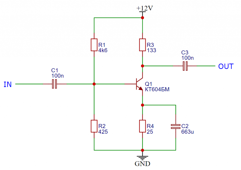
So let’s get started, I figured it would be best if we threw ourselves into a little deeper water right away, so above you can see the schematic diagram of the circuit that works, which we will prepare in a moment. As you can see, the circuit has a separate signal input and output, and the emitter is a common lead for both of them.
The design consists of four resistors, two capacitors and a transistor, and the whole thing is powered by 12V. To begin with, let’s look at the semiconductor element, for testing I chose a Soviet КТ604БМ from 1986. Its Western counterpart is the BF458, but they are not identical designs, they differ in one rather important parameter. In the BF458 the gain is 25 – 240, while in the transistor from the USSR this parameter is in the range of 30 – 120. We must keep this in mind when selecting other circuit components.
Now let’s discuss the resistors. On the input side you can see two such elements – R1 and R2. Their task is to properly polarize the base of the transistor, so that the transistor is always “on”. We know that at the input there will be a sinusoidal signal with a variable amplitude from 0V to xV, the second value does not really matter now. As you will remember from an earlier article, in order for the transistor to start working, or more precisely, in order for current to start flowing in the collector circuit, there must be a voltage of at least 0.7V at the base, measured relative to the emitter. If it is not there, then yes the circuit will work, but only when the sinusoidal voltage reaches more than 0.7V, and we want to control its full range. Therefore, we must somehow boost the voltage at the base, so that even in the absence of an input signal the transistor is already ready to accept it. To do this, we will just use R1 and R2 in a voltage divider configuration, so that there is always the right voltage at the base.
On the occasion of R1 and R2, let’s also discuss the task of C1. Its role is to separate the input signal from the voltage polarizing the base. Professionally, we would refer to this as separating the DC and AC components. The DC component is the small voltage at the base generated by the voltage divider, by definition it is a DC voltage that will not pass through the capacitor. The variable component is our sinusoidal input signal, for it the capacitor is no obstacle, so it will reach the base of the transistor without any problem.
Time for the right side of the circuit and resistors R3 and R4. The role of R3 you have probably already guessed, its task is to control the collector current, so as not to accidentally cause it to exceed its maximum value and burn the transistor. The task of R4, as well as C2, is to ensure proper operating conditions of the semiconductor design at the time, the circuit will not be loaded. The resistor will drain the DC component of the signal to ground, and the capacitor will take care of the variable part. The last element is C3, its use is similar to C1. He, too, has the task of separating the variable output signal from any fixed voltages that will appear in the circuit.
Let’s briefly summarize the whole thing. With the help of the transistor, we will want to amplify a small input signal, obtaining a waveform with higher amplitude at the output, at the same time it should be as close to the original version as possible, devoid of noise. This process will be taken care of by all the components around the transistor, which can be said to tune it in the right way.
Tuning the transistor
We already know how the common emitter circuit is supposed to work, and we also know what we want to achieve with it. So it’s time to select all the components, so as to make the best use of the capabilities of КТ604БМ.
At this point we don’t really know anything about our circuit except that the supply voltage is 12V, but this is already a reference point. To start with, we can try to determine what maximum current can flow in the collector circuit. Looking into the catalog note, we can determine that a maximum of 100mA can flow through the transistor, but we do not want the design to overheat, so let’s take about 80mA as the ICmax value. With such data, we can determine the value of R3 from the formula:
ICmax = (Vcc-UR4-Uce)/R3
Here another problem arises, where to get the value of the voltage drop across resistor R4? The answer may surprise you, but we have to figure out this value for ourselves. However, it cannot be completely random. Let’s consider what happens when the maximum possible current flows through the transistor? It will flow through R3, the transistor and finally R4. The whole thing is supplied with 12V, and this is the voltage that will have to spread across these three elements. The drop for the conducting transistor we know, it is about 0.3V, also 11.7V we must distribute between R3 and R4. At this point, let’s recall what the task of our circuit is. It is to amplify the input signal by both current and voltage. And it is the voltage amplification that is important here, notice where the output is, between the collector and R3, that is where we will need the highest possible voltage. Therefore, the drop on R4 should be relatively small, but also note that a smaller voltage drop means more current will flow through the resistor. We can assume that the voltage drop on R4 will be 1VI think that such a value will be enough to keep the resistor from overheating.
At this point, the formula I referred to earlier simplifies quite a bit, because we have only one unknown, and we can easily calculate such equations.
80mA = (Vcc-UR4-Uce)/R3
(12–1– 0,3)/R3 = 10,7/R3
0,08 * R3 = 10,7
R3 = 133,75Ω
We already know the value of the resistor at the collector, the voltage drops and the maximum current that will flow through this branch. These data will allow us to visualize in a certain way the operation of the transistor on the characteristics.

Each transistor is described by the characteristics of the collector current, associated with the voltage between the collector and emitter, in addition, the base currents are also plotted on the graph. We can plot our results on such a graph, at the same time determining approximately the current as it flows through the base. First, let’s mark the maximum collector current – 80mA, then the supply voltage, which is 12V. The points can be connected by a straight line, which we can professionally call a load line. With it, we can determine the operating point of the transistor, denoted by the letter Q, so it will also be possible to determine the base current. We place the Q point at 40mA, this is simply half of the maximum collector current, this value can also be determined using a formula, let’s check that it is indeed 0.04A.
Icq = (Vcc-UR4)/2/R3
(12-1)/2/133,75
Icq = 0,04A
Looking at the characteristics, we know that the base current will be about 400µA, but what we would really need is an exact value, so we can calculate what resistance R4 should have. Let’s determine the base current from the formula spread below. We also need to assume some value of the transistor’s gain for the calculation. In the catalog note we can find information that the gain is from 30 to 120. So we can safely assume that β is 100.
Ib = Ic/β
0,04/100 = 400µA
Knowing the current that will flow through the base of the transistor, we can calculate the value that the resistor R2 should have. We determine it from the formula below, in which we additionally use the voltage drop at the base-emitter junction. As you remember from the previous material, it is about 0.7V, a standard value for a silicon PN junction.
R2 = (UR4+Ube)/10 * IB
(1+0,7)/10*0,0004
R2 = 425Ω
You are probably wondering why in the denominator we multiply the value of the base current times 10. In general, the theory when we want to properly polarize the base of a transistor, says that the current flowing through the resistors should be quite large, so as not to affect the small values of the IB itself. It is accepted that the current flowing through the second in series resistor should be about ten times the base current.
Once we have determined for ourselves the value of R2, we can determine R1 quite easily. For this we will use the voltage divider formula, in which we multiply the base current by 11, because since 10 x IB flows through R2 it is natural that a value of 11 x IB will flow through the resistor closer to the supply voltage.
R1 = Vcc(UR4+Ube)/11 * IB
12*1,7/11 *0,0004
20,4/0,0044
R1 = 4636Ω
We only have R4 left to calculate, but, to determine its value, we still need the emitter current. Its calculation is quite simple.
Ie = Ic+Ib
0,04+0,0004
Ie = 40,4mA
We determine R4 from ohm’s law by dividing the drop across this resistor and the current flowing through it.
R4 = UR4/Ie
1/0,0404
R4 = 24,75Ω

Well we have almost everything, but we also have to deal with the issue of selecting capacitors. As I mentioned earlier, the task of capacitors C1 and C3 is to separate the variable component from the signals ensuring correct polarity of the transistor. In this article, however, we will not give special consideration to them, however, we are not building a professional audio amplifier. You can only remember that the greater the capacitance of these capacitors, the greater the amplitude of the signal will be, but you can not overdo it, because as the capacitance increases, we lose quality and, consequently, the signal at the output may no longer resemble the input signal. In the circuit being run, I chose ceramic capacitors of 100nF as C1 and C3.
Slightly more attention will be paid to capacitor C2. Its task, like resistor R4, is to dissipate the current flowing through the transistor to ground. However, as you know, capacitors placed in series in DC circuits will never pass current, in which case, what is it for? Remember that the input signal will be in sinusoidal form, and therefore we need an element that will be able to dissipate any signals with a variable component to ground. With such a signal, the capacitor will cope without a problem. We determine the value of the capacitance of this element from a simple assumption – the reactance of the capacitor should be about 1/10 of the value of the resistor at the emitter, so around 2.4Ω. Knowing the reactance, we can apply the formula shown below and calculate the value of C. For f we take the lowest value of the frequency of the input signal at which our circuit should operate, I inserted here 100Hz.
Xc = 1/(2πfC)
2,4 = 1/(2*3,14*100*C)
2,4 = 1/628C
C = 663µF
Let the transistor speak

Once the circuit is ready, it can be put into operation. Ne input I gave a 10kHz sine wave signal, simultaneously connecting two oscilloscope probes, so that the CH1 waveform corresponds to the input, and CH2 to the output. In the photo above you can see what both signals look like.
On the input we see a nice sine wave with an amplitude of about 400mV and a frequency of 10KHz. On the output, the signal has the same frequency, but its amplitude is already about 2V. As you can see, the circuit works, and, importantly, it amplifies. It is also worth remembering that in the common emitter circuit the signal at the output is inverted, in fact shifted by 180°, which is a characteristic of this configuration.
How does the Soviet transistor КТ604БМ burn?

— Yes
— Sitnikov, you are an engineer , like me. Tell me, please, how does the core of the 604БМ transistor explode? Not how it melts, but how it explodes?
— I don’t know, because I don’t know how it could explode.
I think that with the launch of the common emitter circuit, we can raise another interesting issue related to transistors. The effect of temperature on the way they work. Every electronic component is more or less resistant to temperature, whether it comes from outside or is the result of flowing current. Without much thought, it can be said that at some point the structure will fail, but when does it happen? Also, what happens in a transistor moments before failure? I will try to answer this question in this part of the material.

Temperature dependence of the conductivity of a doped semiconductor. (http://Zależność konduktywności półprzewodnika domieszkowanego od temperatury.)
What happens when the temperature of a semiconductor increases, answering in three words – the current flowing increases. Well, the answer as correct as possible, but it does not exhaust the topic. Therefore, let’s go down to the level of silicon for a moment and examine what actually happens to the transistor as the temperature increases.

Valery Legasov talking about the explosion of the RBMK reactor core. A scene from the Chernobyl series produced by HBO. (https://ew.com/tv/2019/06/07/chernobyl-russia-tv/)
Each transistor is built from properly doped semiconductor material. It can be said that doping is actually the addition of additional energy carriers to the main building block. In an N-type semiconductor this will be electrons, in a P-type it will be holes. At “normal” temperature, i.e. up to about 150°C for silicon and 70°C for germanium, we can easily control all these free energy carriers by applying the appropriate voltage to the leads of the transistor. Just like in the previously launched common emitter circuit. It starts to get more interesting when we exceed the maximum operating temperature.
The first effect of too high a temperature will be vibrations, but ones that we won’t notice with the naked eye. Vibrate, at first tentatively will be single atoms of the material from which the semiconductor is built, for simplicity let’s assume that it is silicon. As the temperature increases, the vibration will also increase, until it exceeds a certain critical point, which will not completely damage the component, but will cause irreversible changes.
The critical point will be the moment when vibrating silicon atoms begin to eject electrons into the space around them, so far moving on the last so-called valence shell. Remember, however, that this space is already full of energy carriers anyway, added in the doping process. The spontaneous appearance of additional electrons causes, one rather serious problem – a decrease in resistance. But let’s assume that at this point we cool the transistor to room temperature. Will it continue to operate, even though its maximum operating temperature has been exceeded? Probably yes, but its parameters may have changed. Unfortunately, we can’t undo the changes that have occurred at the atomic level, because most of the electrons won’t return to their place.
But what happens if we don’t stop the whole process and let the transistor continue working. The decrease in resistance generates another problem – an increase in the current flowing, this in turn increases the temperature even more. At this point, we already have a self-perpetuating process that will continue until there are simply too many energy carriers, and the whole structure through the combustion process will cease to exist.
This is what the effect of temperature on a semiconductor looks like at the atomic level. I have to admit that the description I prepared reminds me a little of the discussion of the RBMK reactor explosion process from the HBO series Chernobyl, which is where the introduction to this chapter came from.
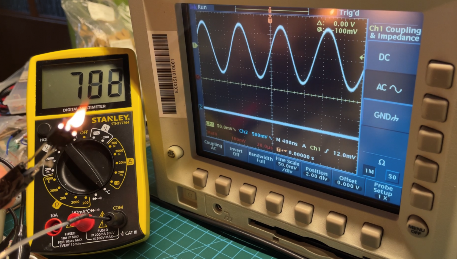
Taking up the topic of temperature and semiconductors, I decided to do simple practical tests, the result of which you can see above. I ran a common emitter circuit, identical to the one before, except that the transistor was placed outside the contact board. On the oscilloscope you can see the input signal (CH1) and the output (CH2), the approximate temperature is displayed on the multimeter.
As you can see, as the temperature increases, the amplitude of the output signal decreases. Not surprisingly, more and more energy carriers appear, the current increases, resulting in a decrease in voltage. It can be said that the limiting temperature is about 550°C, after exceeding this value the signal completely disappears. Although, as you can see, КТ604БМ is not damaged and after cooling the signal returns, even repeatedly. I am surprised that the design withstood, as much as such temperatures, in the catalog note we can find information that the transistor should work in the range from -60°C to 100°C.
In the second test, I decided to take the КТ604БМ to the edge of its capabilities, that is, to literally set it on fire. As before, the output signal disappears after exceeding about 550°C, but this time it deals with a living fire and reaches almost 800°C at one point. Such a temperature, however, turns out to be already too high, the transistor dies, and the output signal does not return.

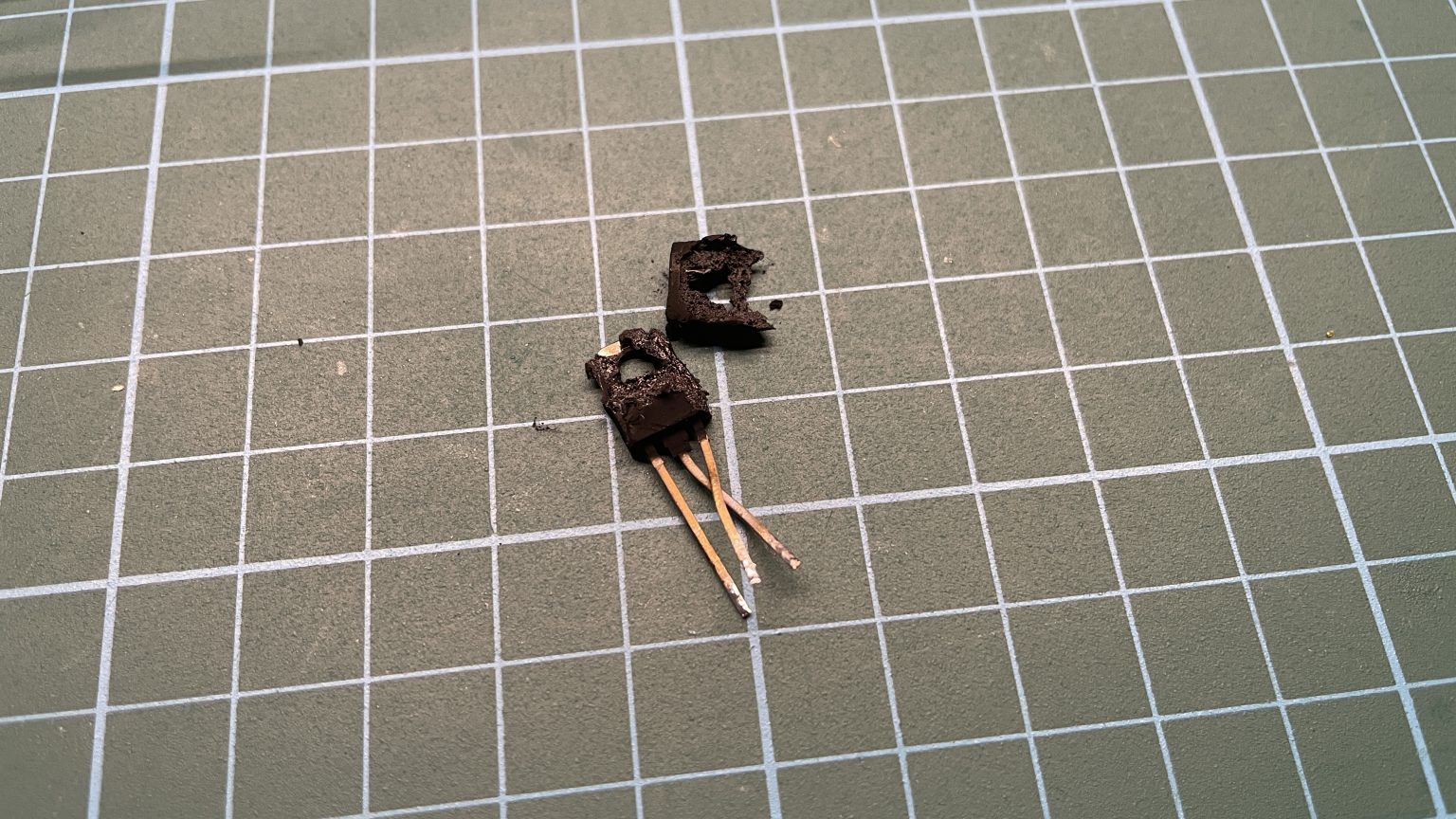
After the last test, it turned out that the charred transistor housing had disintegrated into two parts. This is how semiconductors whose temperature exceeds the acceptable operating range can end up.
Sources:
- https://eandc.ru/pdf/tranzistor/kt604.pdf
- https://datasheetspdf.com/pdf-file/1293292/Toshiba/BF458/1
- https://www.electronics-tutorials.ws/amplifier/amp_2.html
- https://studylibpl.com/doc/1120699/wp%C5%82yw-temperatury-na-p%C3%B3%C5%82przewodnik-oraz-na
- https://rafalbartoszak.pl/narodziny-zycie-i-smierc-tranzystora/
