- Is the LED in the optocoupler actually lit?
A transoptor, which is a creative combination of a transistor and an LED, is not one of the basic electronic components. It is not as common as resistors and capacitors, but it has found its niche in specific types of applications, mainly due to its unique design.
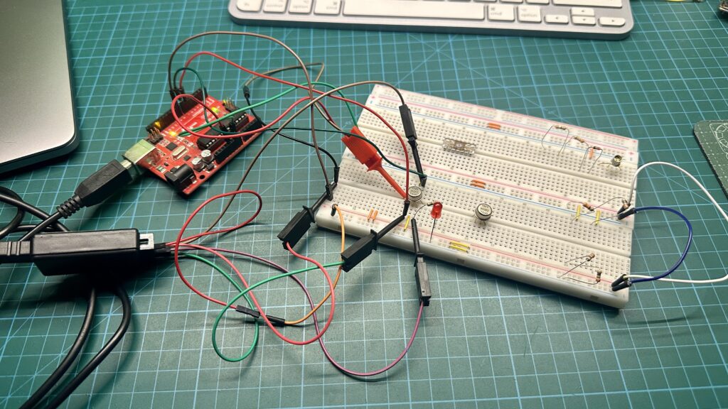
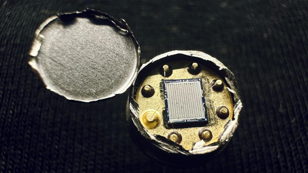
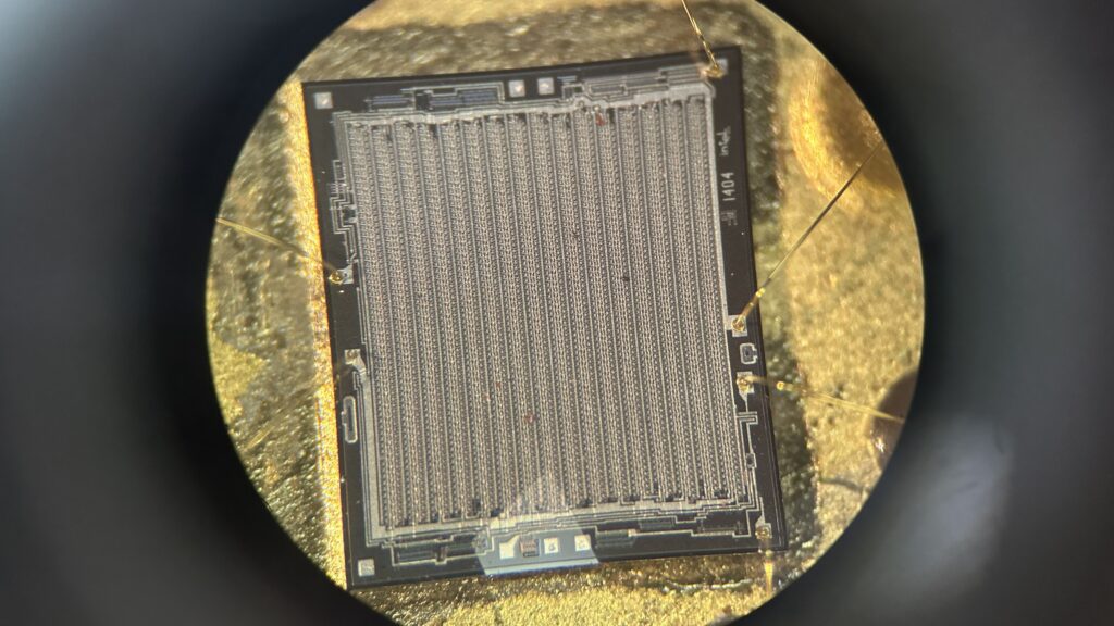
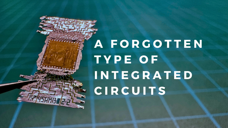
- The mysterious electronic module and the first Soviet integrated circuits
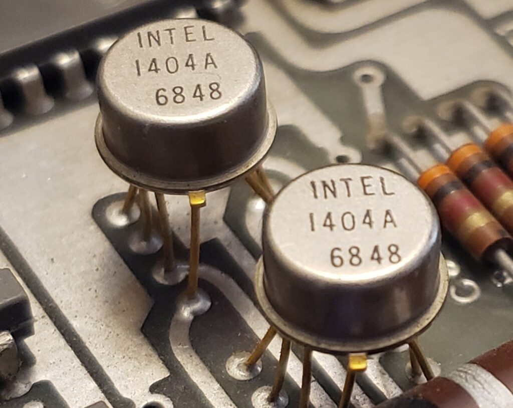
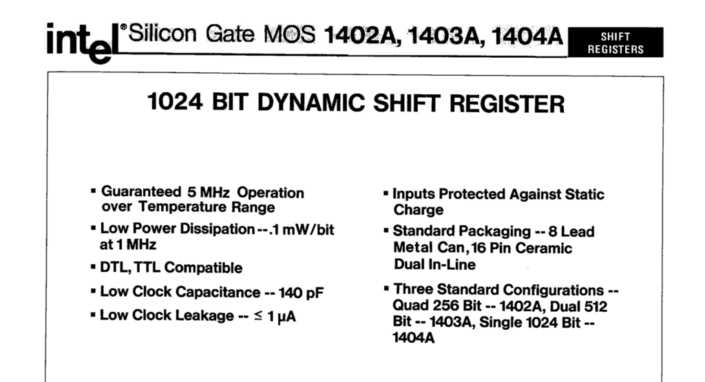
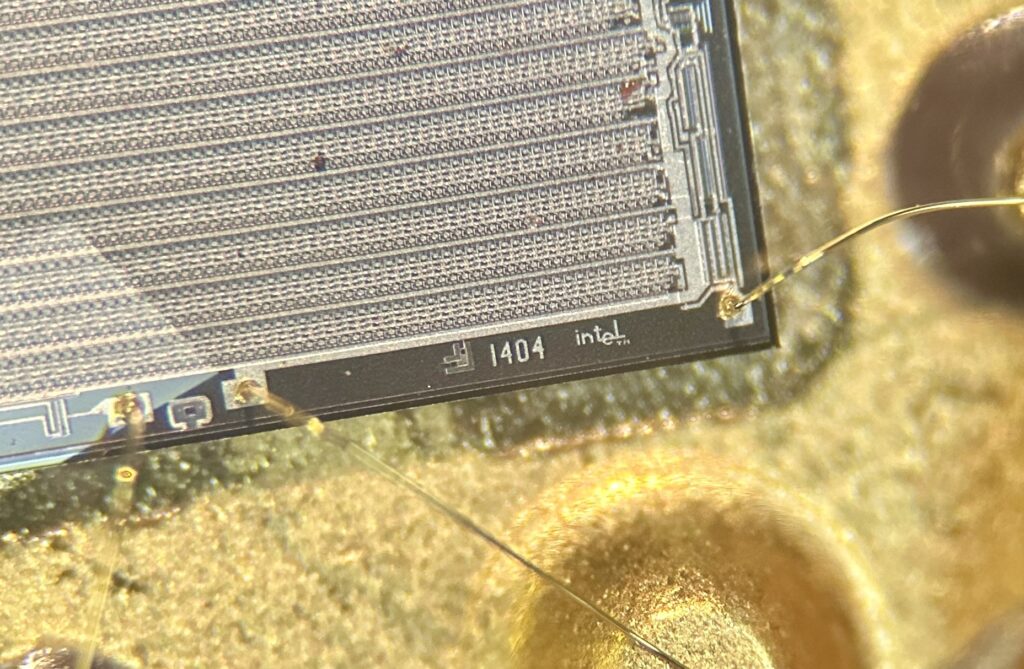
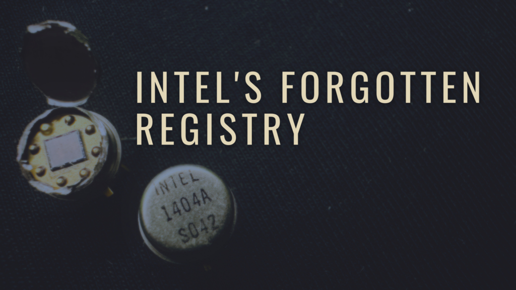
In the package with electronic equipment from Mr. Marek, apart from an interesting Intel chip, which was mentioned in an article some time ago, there was also a mysterious module, and that is what we will focus on today.
- STM32 Ethernet – UDP Client
Recently, I had the opportunity to work on a project using an STM32 microcontroller and an Ethernet interface. Like others who have tackled this topic, I encountered a problem – the lack of “simple” guides. In most of the available sources, connecting the Ethernet interface and STM32 chips is described in a rather confusing way, and in my opinion, there is a lack of instructions describing how to configure this functionality in the simplest possible way, without unnecessary exploration of network aspects. That is why I decided to prepare this and related materials on the subject of Ethernet on STM32. In this article, I will show you the basic functionality of a UDP client. That is, code whose operation is, in a sense, the opposite of a UDP server. In the previous tutorial, the STM32 acted as a server to which the computer connected, this time we will create a server on the computer to which the microcontroller will connect.
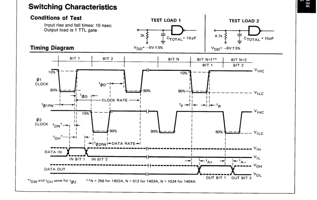
- Miniature clock with retro integrated circuit
Rumor has it that the only silicon structures that Polish engineers interfered with were clock circuits. It is difficult to confirm this, however, as it is known that factories in communist Poland produced silicon from ready-made designs, but not much is known about our native designs. At that time, technologies of this type were quite well protected, but who knows, there is a grain of truth in every rumor. Miniature clock with a retro integrated circuit
- MS1 – simple soft processor on FPGA
Everyone has thought about building their own processor at some point, well, maybe not everyone, but I happen to be in that small group of people. Almost from the very beginning of my interest in electronics, I was most fascinated by its digital aspects, and although programming was much more impressive, I enjoyed designing logic circuits the most. In the past, I built various designs that could be called simple processors or microcontrollers, depending on the solutions used. These devices were based on basic logic circuits, and although they were impressive at the time, over time their expansion became increasingly difficult and expensive, especially for someone who had just started high school. Wanting to learn more about the secrets of digital technology, I had to go a step further, and that's how I became interested in programmable circuits. This led to the creation of new designs based not on many separate chips, but on a single piece of silicon enclosed in an FPGA. However, I will talk about them, as well as the older, logical designs, in another article, because the subject of this text will be one of my most recent projects.