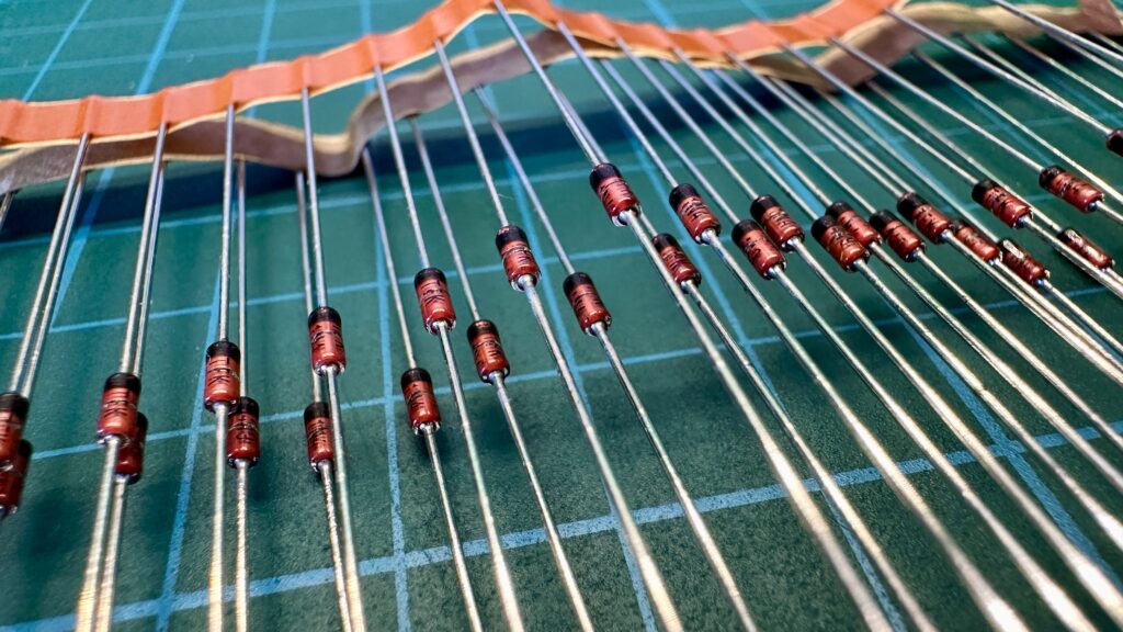
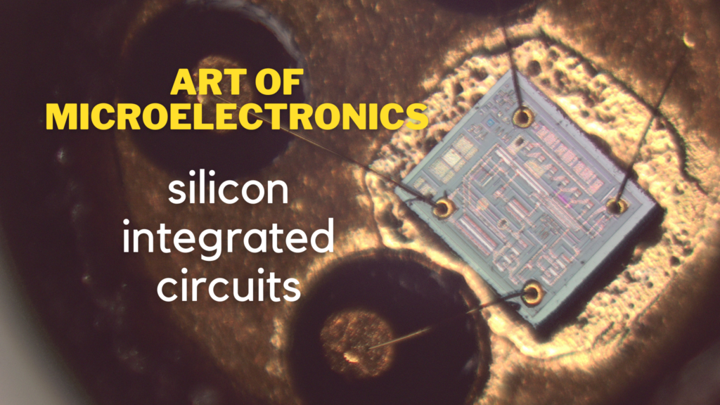
Modern microelectronics is one of the fastest growing areas of science and technology. Its relevance to our daily lives is immense, as it is thanks to microelectronics that we can use advanced electronic devices, such as smartphones, tablets and laptops, which have become an integral part of our reality. In today’s article, we invite you to take a deeper dive into the fascinating world of silicon, where we will consider the construction of elements such as transistors and diodes.
Semiconductor diode in a semiconductor

Semiconductor diodes are extremely important elements in the world of electronics and are one of the basic components of integrated circuits. Their role in electronics cannot be overestimated, as they not only act as rectifiers, but are also used to generate signals, convert electricity and even as surge protective elements. Thanks to their ability to conduct electricity unidirectionally, diodes allow controlled operation on electrical circuits, which is essential in most electronic devices.
The designers of the rectifier diode based the entire design on two layers of semiconductor with different properties. The first layer is a P-type material, while the second is an N-type semiconductor. The operation of this type of semiconductor sandwich is based on the flow of electric current in one direction only, the flow in the other direction is blocked unless the diode’s breakdown voltage is exceeded. When this element is polarized in the right way and the voltage applied to the diode is greater than the threshold voltage (the conduction voltage), the current is passed through, allowing the rectifying diode to use only one half-period of the alternating signal, rectifying it into a unidirectional form.

Typically, semiconductor diodes come in the form of individual components mounted on PCBs. However, it is worth knowing that such structures are also built on silicon substrates in integrated circuits. In the photo above you can see the core of a circuit manufactured by Warsaw’s CEMI plant with the designation UL1520. This is a voltage converter, on the input of which there are placed, connected in series, four zener diodes and six semiconductor diodes, I marked them in the photo with a black rectangle.
It is quite easy to see that there are two paths connected to each diode, being its input and output. However, upon a slightly closer look, the whole structure may seem a bit strange. Quite clearly, each diode is actually connected to a metal path in three places, with two of the leads connected to each other. It might seem that there are no simpler silicon structures than rectifier diodes; after all, it was based on just two layers of semiconductor material. The reality is somewhat different, however, and it is quite common to build diodes from transistor structures.
We’ll get to the transistors themselves a little later, but the graphic interpretation of the diode’s construction in silicon that you can see above shows the de facto certain transistor from which the diode was made. You are probably wondering why this is so? The answer is quite simple, it’s all about technology. The analyzed chip was made in TTL (transistor-transistor logic) technology, and that’s why the diode was made from a transistor, if the chip was made in DTL, (diode-transistor logic) convention the silicon structure would have a slightly different structure.
But let’s move on to a concrete description of the structure of the diode on a silicon substrate. As you already know, here we have a transistor structure with three leads. On the right side, the N+ area was placed, which plays the role of an N-type semiconductor in a classic rectifier diode. A metal lead – the cathode – was also placed here. The N+ material is placed inside a larger P-type area to which the middle lead (of the transistor) is attached, it is connected to the metal on the left connected to an even larger N+ and N-type area. The inner P-type semiconductor is just the second part of the sandwich, which is a component of the rectifying diode, and the output connected to it acts as – an anode. The output on the left side, although connected to the anode, in the case of the diode is of little importance, it can be said that it only improves the characteristics of the element, isolating its structure from the rest of the semiconductor substrate.
Bipolar transistors

How a bipolar transistor is constructed hardly needs to be introduced to anyone. In theory, we have a structure built from an appropriately doped semiconductor, arranged in an NPN or PNP type sandwich. Thus constructed, the element allows to amplify and control the flow of current between two of its leads. Typically, we can meet transistors as three-lead elements that are part of larger electronic circuits. Besides, transistors are the basic building blocks of integrated circuits, it is on these elements that all modern integrated circuits are based. However, it is worth knowing that their construction on a silicon substrate differs significantly from the theoretical three-layer PNP or NPN sandwich.

In practice, NPN-type bipolar transistors are formed from several layers of P-type, N-type and N+ semiconductor. The entire structure is placed on a P-type substrate and has little in common with a book NPN, although looking at the vertical slice below the emitter, we can see such a structure. Below the emitter is placed an N+ type semiconductor, it connects directly to the P area, which is the area connected to the base. The last element is the collector, it connects to the rest of the structure indirectly, that is, two N+ areas are separated by an N-type semiconductor.

One would expect a PNP transistor to be built identically to an NPN, with the difference being only the reverse designation of the semiconductor type. The reality, however, is different. PNP transistors have a small, usually circular P-type emitter region surrounded by a collector ring, also P-type. The two areas are separated by an N-type semiconductor, connected indirectly to a slightly more doped base, N+. In the picture you can see a rather interesting transistor, in which between the base and the collector passes a path placed above the whole structure, on a layer of silicon oxide.
Unipolar transistors
In addition to bipolar transistors in electronics, we can also encounter unipolar designs, also known as field-effect transistors. These types of components use the phenomenon of an electric field to control the flow of electric current, which makes them extremely versatile and efficient components. Like bipolar transistors, field-effect designs are among the basic components used in the semiconductor industry.

Unipolar transistors are among the simpler designs in terms of construction. Elements labeled NMOS and PMOS, or N-type and P-type channel transistors, respectively, are built on silicon substrates. In the graphic above you can see the general construction of two MOS transistors on an N-type substrate. In the design on the left at the drain and source junctions, P+ type areas have been placed, separated by a channel with a baseline of more electrons, above which a gate has been placed. As in classical through-hole components, it is separated from the substrate by a thin insulator layer. The housing of the P-channel transistor (on the right) is almost identical, except that the semiconductor materials used are, so to speak, reversed. In other words, an N+ type region was placed under the drain and source, while the whole structure was placed in a larger P-type region, so as to obtain a channel with such characteristics under the gate.
In the graphic you can still notice a mysterious lead marked B, connected to the source of the transistor. It is necessary for the proper functioning of MOS transistors placed on a silicon substrate. Such elements require that the transistor site is polarized with a voltage from the source. This prevents the signals switched by the transistor from “escaping”, in other words, a bubble is formed around the transistor, so that it is somehow isolated from the rest of the silicon structures placed on the same substrate.
The modern world is constantly flowing toward the future, driven by incredible advances in technology. Central to this dynamic process is the electronics that underpin most everyday devices. One of the key foundations of electronics are structures called integrated circuits, which have been revolutionizing our ability to process information and communicate for years. However, when we look deep into electronic chips, we see that they are made up of structures such as transistors, diodes, resistors and even capacitors. These elements are placed together, on a single piece of silicon, which makes them significantly different from similar structures placed on printed circuit boards. In this article I will tell you a little about silicon electronic structures, the foundation of today's technological world.
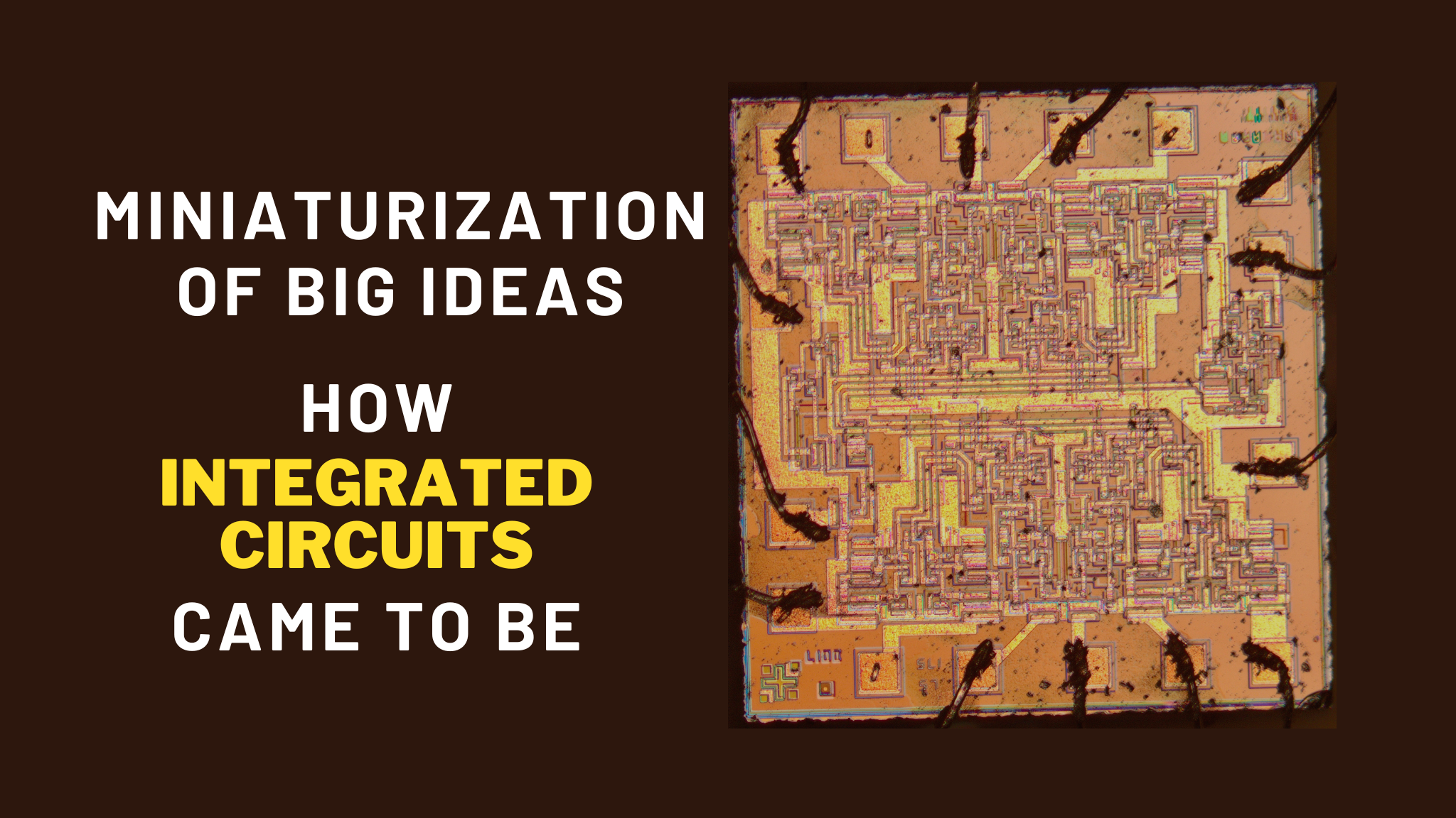
In today's dynamic world of electronics, we are constantly using advanced technologies that enable us to perform tasks faster, more efficiently and more conveniently. One of the most remarkable developments that has affected our daily reality is the invention of the integrated circuit. These small but powerful electronic components, typically containing hundreds, thousands or even millions of elements on a single silicon wafer. Chips have revolutionized our world in ways we could not even imagine before. But in order to explore the history of integrated circuits, we need to go all the way back to the 1920s, to the days of tube designs.
Sources:
- https://www.shindengen.com/products/semi/column/basic/diodes/diode.html
- https://www.elenota.pl/datasheet-pdf/60410/CEMI/UL1520?sid=f990c1328e28e9c37bed32e0d18712b7
- http://www.righto.com/search?q=diodes&updated-max=2020-07-25T09:51:00-07:00&max-results=20&start=6&by-date=false
- http://www.righto.com/search?q=cmos+diode&updated-max=2021-03-03T10:16:00-08:00&max-results=20&start=3&by-date=false


