ALUs, or arithmetic logic units, are part of every processor today. In the past, they were produced as single, physical chips or a collection of multiple logic chips. In today’s material, I will tell you about the construction, history and operation of one of the first ALUs.

The main role in today’s story will be played by a chip designated 74181. It is a TTL chip enclosed in a 24-pin housing, first presented to the world in early 1970 by Texas Instruments. The chip is a full-fledged arithmetic and logic unit enclosed in a single housing. It can add, subtract and perform any type of logic operation.
The 74181 consists of 75 logic gates, making it a medium-scale integration circuit – MSI. It does not need a clock signal to work, because it is built as a combinational chip, in which two 4-bit operands are processed according to a 4-bit command. The chip has no memory, so in larger designs it always had to come in tandem with additional registers, called “accumulators.”
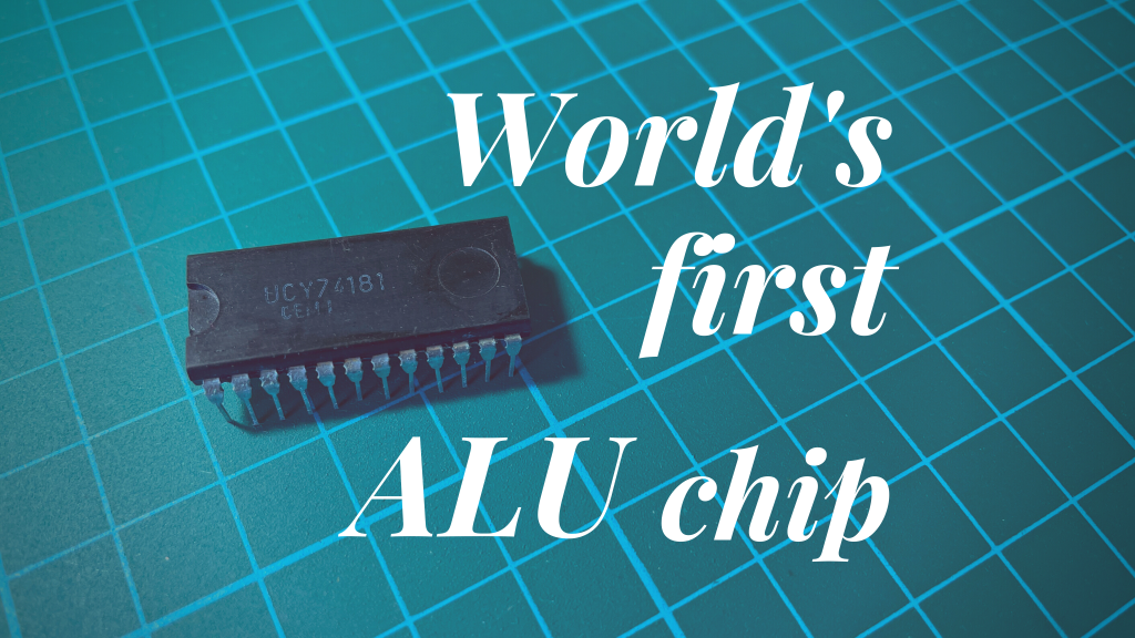
Interestingly, the 74181 was also produced in Poland by Warsaw’s CEMI plant. At that time it bore the name UCY74181. You can see the “Polish-made” ALU in the photo above.
Was 74181 the first ALU?

Nova 1200 computer processor – possibly the first hardware using the 74181 (https://apollo181.wixsite.com/apollo181/about)
Was the 74818 the first ALU chip? One can answer that yes, but, as is often the case in electronics, such an answer does not exhaust the subject one hundred percent, and much depends on what we actually mean by the term ALU. The history of arithmetic-logic units actually begins two years before the introduction of the 74181 in 1968, and in order to understand the subject properly we need to familiarize ourselves with several different circuits.
- September 1968 – 4771 – An accidental ALU from Fairchild that never went into production.
- November 1969 – N8260 – First very simple ALU released by Signetics.
- March 1970 – SN74181 – 4-bit ALU with support for 32 operations (Texas Instruments).
- March 1970 – 9341 – chip compatible with 74181 (Fairchild).
- August 1970 – F9340 – a simpler version of the 9341/74181 (Fairchild).

The PERQ workstation, introduced in 1980, was probably the last commercial machine based on the 74181 chip (https://apollo181.wixsite.com/apollo181/about)
The late 1960′s saw a constant technological race between the semiconductor giants of the time. At the time, companies such as Fairchild and Texas Instruments had the technologies to “rapidly” design and put into production new types of circuits. At Fairchild, the process was called Micromatrix, while at TI it was called Discretionary Routed Arrays. Of course, we must take the word fast with a pinch of salt; the design process took months, but it was faster compared to classic technologies. Both manufacturers relied on off-the-shelf logic arrays, in which any connections could be made between the gates placed on it. This type of board had 48-96 logic elements as standard, which is a relatively small number, especially compared to today’s integrated circuits, but in its time a fully functional chip could be designed on such a board.
The first chip that we can describe as an arithmetic-logic unit was created in September 1968. Manufactured at the Fairchild plant, the chip, designated 4771, was not really a response to market needs, but only a demonstration of the possibilities. Engineers wanted to prove that Micromatrix technology could create a more customized yet advanced chip. Thus, a simple 4-bit ALU was created, which never achieved success primarily through performance problems with the operations performed.

Signetics 8260 chip (https://apollo181.wixsite.com/apollo181/about)
The first chip to be marketed that we can, stretching the definition, refer to as an ALU is the N8260, designed in November 1969 by Signetics. This chip could only perform three operations – addition, logical AND and logical XNOR, also referring to it as an arithmetic-logic unit is a slight stretch. The N8260, like an earlier invention from the Fairchild stable, will not achieve much success, and I suspect that this may have been due, among other things, to the unconventional physical form of the chip, which you can see in the photo above. It should be mentioned, however, that the Signetics-designed design is the only chip mentioned by Texas Instruments in its documents on the 74181.
In March 1970, Texas Instruments entered the game by showing the world a real ALU, the 74181 chip. Although it was released in early 1970, the first mentions of it appear as early as August 1969 in the “TTL Integrated Circuits Catalog from Texas Instruments,” three months before the N8260 was launched. TI’s design proved to be a success, despite initial performance problems, resolved in 1971, after the switch to so-called “Schottky TTL” technology.

First version of the 9341 chip. (https://apollo181.wixsite.com/apollo181/about)
It didn’t take long for other technology companies to respond. Later that same month Fairchild releases the equivalent of the 74181 under the name – 9341. A few months later, in August 1970, the company tries to conquer the market with a simpler version of the chip from TI. But the F9340, as it was released under this name, does not achieve much success.
How does the 74181 work?

Prior to the introduction of the 74181 chip, each arithmetic-logic unit was realized by a collection of more or less advanced circuits, forming together larger functional blocks, such as adders. However, when we look at the internal schematic of today’s hero available in the catalog note, we can conclude that something is wrong here. Considering the supported operations, we would rather expect specific blocks performing specific functions, yet we see a rather simple circuit, with somewhat haphazardly arranged gates.

Internal construction 74181 (https://www.ti.com/lit/ds/symlink/sn54ls181.pdf?ts=1655469418863&ref_url=https%253A%252F%252Fwww.google.pl%252F)
One of the simplest ways to perform addition is to use one-bit adders for each bit. Such an operation is based on transfers and is actually very slow. For example, when adding 9999 + 1, the adders must send a one through each adder, one at a time. The result is that our addition is a serial, nonparallel operation which has a negative impact on the performance of the ALU. To solve this problem, the designers of the 74181 decided to designate the carry bit first, and only then perform the addition. Such a solution may seem rather strange, because how can you generate the carry bit before performing the addition? However, it turns out that it is possible.

Circuit generating ‘G’ and ‘P’ signals (https://www.righto.com/2017/03/inside-vintage-74181-alu-chip-how-it.html)
The transfer in 74181 is actually based on two internal signals ‘G’ and ‘P’ (Generate and Propagate). They are created based on the input, without taking into account the result of the operation, and determine whether the transfer should potentially be generated. For example, if I add 0+0+C (where C is the input of the transfer) I have no possibility of getting a positive transfer in the output. Similarly, performing the operation 1+1+C the transfer will always have the value ‘1′. Finally, for 1+0+C or 0+1+C, the positive carry at the output depends entirely on the input carry bit, taking its value. In summary, the chip sets the value of ‘G’ if both bits have the value ‘1′ and the signal ‘P’ if any input signal takes the value ‘0′.

Features supported by the 74181 (https://www.ti.com/lit/ds/symlink/sn54ls181.pdf?ts=1655469418863&ref_url=https%253A%252F%252Fwww.google.pl%252F)
The 74181 supports 16 logic functions and 16 arithmetic functions that depend additionally on the transfer input. Taking a closer look at the logical operations, we will not see anything strange, just standard operations, it is different with arithmetic functions. Some of them are quite strange, one could say overcomplicated, for example, A PLUS AB PLUS 1. However, here, too, behind everything there is a certain system and a thoughtful action of the circuit developers.
Arithmetic functions are actually based on logical ones, that is, the variable ‘A’ was added to the 16 logical commands along with the transfer. Let’s take the previously mentioned A PLUS AB PLUS 1, if we decompose this operation into its first parts, we actually get A PLUS (logical F=AB) PLUS C.
What is hidden inside?

Silicon core of the 74181 chip (https://www.righto.com/2017/01/die-photos-and-reverse-engineering.html)
No material of mine can do without a look inside the device or circuit. In the photo above you can see the core of the 74181 chip. It is based on a substrate made of silicon, barely visible indistinct lines allow you to separate the more or less doped areas that make up the transistors and resistors. On the silicon there are white/gold stripes, made of aluminum, connecting individual circuit elements. At the edges we can also find white squares – pads, to which small wires are attached, connecting the silicon with the chip’s leads.

The 74181 was made using TTL technology, meaning it is based primarily on bipolar transistors. Nowadays, circuits are mostly based on MOS-type elements. The structure of bipolar transistors, rather, does not need to be introduced to anyone. In theory, we have a structure built from an appropriately doped semiconductor, arranged in an NPN or PNP type sandwich. In reality, bipolar NPNs are formed from several layers of P-, N- and N+-type semiconductor. The main difference between the N and N+ areas is the amount of doping, N+ being a richer, more doped semiconductor. The whole structure is placed on a P-type substrate and has little in common with the book NPN, although looking at the vertical slice under the emitter, we can see such a structure. An N+ type semiconductor is placed under the emitter, and it connects directly to the P area, which is the area connected to the base. The last element is the collector, it connects to the rest of the structure indirectly, that is, two N+ areas are separated by an N-type semiconductor.

NOT gate (https://www.righto.com/2017/01/die-photos-and-reverse-engineering.html)
One of the basic logic components is a NOT gate, egg the task is simple invert the input signal. Above you can see the construction of such a gate in the 74181 chip. The individual transistors are marked with colored rectangles, while the power lines run vertically, at the left edge of the silicon slice.
The gate input is connected to transistor Q1. This element is used in a rather unusual way, it acts as a “current control” transistor. If the input is given a low state, the current flowing through R1 is directed through the emitter (Q1) to the input, leaving Q2 off. If the input takes the value of logical ‘1′, the current of R1 flows “backwards” from the collector of Q1 to the base of Q2, turning Q2 on. Transistor Q2 can be thought of as a ‘phase splitting transistor’, which ensures that exactly one of the output transistors (Q3 or Q4) is activated. This means that they turn on in opposite phases. If Q2 is off, R2 provides the current to turn on Q3, resulting in a high state at the output. Meanwhile, R3 turns off Q4. On the other hand, if Q2 turns on, it provides enough current to turn on Q4, so that we have a low state at the output.

XOR gate (https://www.righto.com/2017/01/die-photos-and-reverse-engineering.html)
It must be admitted that compared to the NOT gate, the XOR construction is extremely poor. But as Leonardo da Vinci and later Steve Jobs used to say – “Simplicity is the height of sophistication”. The gate was based on two transistors connected in a rather unusual way, the collectors are common, and the bases are connected to the emitters. It is also worth noting that there is no ground in the circuit.
The way it works is that if you give ‘1′ to the first input and ‘0′ to the second input, the first transistor will be triggered by the base-emitter current. This will make the voltage at the output disappear, and the second input will act as ground. Similarly, if we polarize the first input negatively and the second input positively, the second transistor will turn on and lower the voltage at the output. If identical base-emitter current voltages are applied to the inputs, and both transistors remain off, then the output is pulled up to logical one by a resistor.

“NOT-AND” design (https://www.righto.com/2017/01/die-photos-and-reverse-engineering.html)
The 74181 is based largely on AND gates, but four of them, which are indistinguishable on an ordinary schematic, are built in a slightly different way. The unique gates are so-called “NOT-AND” structures in which one of the inputs is negated.
At first glance, the design looks ordinary, transistor Q1 is connected normally with resistor R1 at the base, but Q2 has its resistor connected to the collector, not the base. Normally, R2 will pull up the output signal to one, but if we give ‘1′ to the X input and ‘0′ to Y, the current of R1 will flow through the collector of Q1 and the emitter of Q2. The effect will be to turn on Q2 and lower the voltage at the output. Thus, at the output of our AND gate there will be a logical one, only if X is in the ‘1′ state and Y – ‘0′.

Diagram of 74181 with marked areas (https://www.righto.com/2017/01/die-photos-and-reverse-engineering.html)
The schematic of the 74181 chip is also quite interesting, with the areas of the individual logic blocks marked. An analogous schematic only applied to the silicon core of the chip you can see below.

Silicon core with marked gate areas (https://www.righto.com/2017/01/die-photos-and-reverse-engineering.html)
Sources:
- https://apollo181.wixsite.com/apollo181/about
- https://www.ti.com/lit/ds/symlink/sn54ls181.pdf?ts=1655469418863&ref_url=https%253A%252F%252Fwww.google.pl%252F
- http://www.righto.com/2017/03/inside-vintage-74181-alu-chip-how-it.html
- http://www.righto.com/2017/01/die-photos-and-reverse-engineering.html