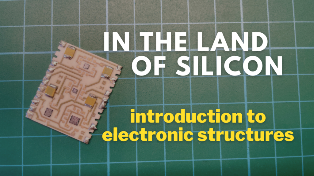
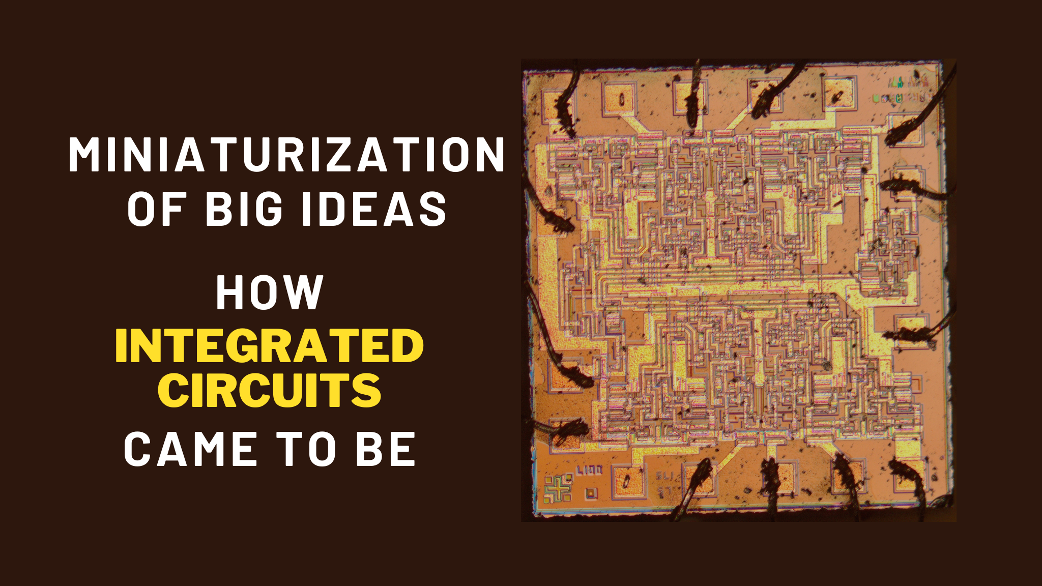
The modern world is constantly flowing toward the future, driven by incredible advances in technology. Central to this dynamic process is the electronics that underpin most everyday devices. One of the key foundations of electronics are structures called integrated circuits, which have been revolutionizing our ability to process information and communicate for years. However, when we look deep into electronic chips, we see that they are made up of structures such as transistors, diodes, resistors and even capacitors. These elements are placed together, on a single piece of silicon, which makes them significantly different from similar structures placed on printed circuit boards. In this article I will tell you a little about silicon electronic structures, the foundation of today’s technological world.
A quick course on building integrated circuits
In the previous material linked above, I briefly introduced the history of integrated circuits, but in order to better understand their internal structure, it is advisable to learn about “chip theory.” Integrated Circuits (ICs) are electronic components in which many small components, such as transistors, resistors, capacitors and others, are placed on a single thin semiconductor substrate, usually silicon. Building an integrated circuit is an extremely precise process that allows hundreds of thousands or even millions of components to be placed in an area smaller than a fingernail. There are different types of integrated circuits, including analog, digital and hybrid, depending on the type of components and the functions they perform.
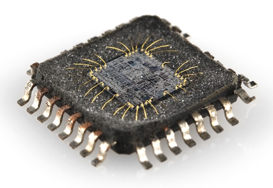
The construction of modern monolithic integrated circuits, for such we will primarily be concerned with, can be described in a few sentences. The core of the chip, usually placed on a slightly larger metal or ceramic substrate, is enclosed in a hermetically sealed housing made of plastic, or ceramic material. External leads are placed on the edges of the enclosure, their arrangement and number depends on the specific type of enclosure. The core of the circuit and the leads are connected by thin, usually gold wires, which are attached to the surface of these elements by ultrasonic or welding methods.
Why silicon?
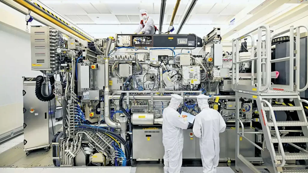
Anyone with an interest in electronics knows that a significant portion of semiconductor components are made from silicon, with most having probably also heard of germanium designs, but not used them. Both materials are used in today’s world, but the importance of germanium is actually marginal, and it is silicon that dominates the high-tech market. This has happened for several practical reasons:
- Availability and cost: Silicon is the second most common element on earth after oxygen. It is available in large quantities and is relatively easy to mine. This makes it much cheaper than germanium, which is found in smaller quantities and is more difficult to obtain.
- Thermal stability: Silicon has excellent thermal stability, which means that integrated circuits made from this material can operate over a wide temperature range. For advanced technology processes, this is important because chips must operate not only at typical room temperatures, but also under extreme conditions, such as in industrial or space applications.
- Silicon oxide as an insulator: Silicon oxide (SiO2) has excellent insulating properties, making it an excellent material for creating insulating layers in MOSFET transistors. The insulating layer separates the gate of the transistor from the conduction channel, which is crucial to its operation. Silicon oxide can be formed simply by oxidizing silicon, which is a durable and reliable process.
- Developed manufacturing technology: Silicon-based IC manufacturing technology has been highly advanced and developed for decades. Much investment, research and development has been devoted to perfecting the technological processes involved in silicon chips. As a result, silicon chips offer excellent performance, low power loss, and the ability to integrate hundreds of millions of components on a single core.
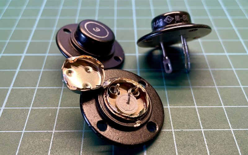
Opening germanium transistors, especially those from the Soviet Union, is not the best idea, because the interior of such structures was filled with beryllium oxide, which is a dangerous element. Its purpose was to improve heat dissipation in the transistor.
In addition to the obvious advantages, there is one issue in which germanium semiconductors excel over their silicon competitors, and that is electrical properties. Electrically, germanium can be described as a superior element, characterized, among other things, by higher electron mobility. This term refers to the ability of energy carriers to move freely in a material. This property affects a number of characteristics of germanium semiconductors, but this is an issue that I will perhaps address in another article.
Doping - the secret ingredient for success
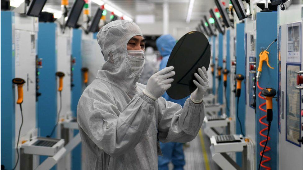
Learning about the theory of semiconductor structures, we usually stop at the information that, for example, transistors are built from appropriately doped silicon, in which N- and P-type areas are formed as a result of this process. Well, this sentence is as true as possible, but, as is usually the case, it does not exhaust the subject. Wanting to know the world of microelectronics, we need to know semiconductors a little better.
The process of doping semiconductors, involves the controlled introduction of small amounts of dopant atoms into the crystal structure of silicon. The process is designed to change the electrical properties of the semiconductor, such as conductivity, type of conductivity and mobility of charge carriers. Doping is a key step in the production of semiconductors, as it controls the electrical behavior of the material and makes it possible to create different types of semiconductor components, such as transistors and diodes.
The basic types of dopants are the previously mentioned, P-type acceptor dopants and N-type donor dopants. P-type dopants are substances that have fewer electrons in their structure than the semiconductor into which they are introduced. This means that when introduced into a semiconductor, electrons will be in short supply and not all energy bands will be filled. This results in the formation of so-called “holes”, which act as charge carriers in this type of semiconductor. N-type dopants are substances that have an excess of electrons in their structure compared to the semiconductor. When they are added, excess free electrons are created, which from now on become charge carriers of the opposite sign to the “holes.”
In addition to the basic N- and P-type dopants, we can also distinguish types: N+, N- and P+ and P-. As you can easily guess, these are dopants characterized by a different concentration of charge carriers than the standard. N+ and P+ areas are distinguished by very strong doping, this means that in N+ there are much larger amounts of electrons than in a standard N-type semiconductor. Similarly, in the P+ areas, the dominant elements are “holes,” which are more abundant than in a classical P-type semiconductor. N- and P- areas, are doped with very few invading elements, in other words, they are areas of low concentration of energy carriers. N-type semiconductors are characterized by a much smaller number of electrons compared to N-type areas, while in P-type structures the number of “holes” is significantly smaller compared to P-type areas. This type of redundant or poorer doping is intended to create areas with a specific concentration of charge carriers, which is important in some applications such as Schottky diodes, power transistors and solar cell components.
By default, N- and P-type dopants and their variations introduce excess electrons or deficiencies of this type of charge, or “holes,” but there are other dopants that can have a variety of effects depending on the type of semiconductor and conditions. We can distinguish several such structures.
- Insulating dopants: Introduce dopant atoms that can change the dielectric properties of a semiconductor. This makes it possible to create insulating layers that separate different areas of an integrated circuit.
- Ferromagnetic dopants: With these, ferromagnetic properties can be imparted to a semiconductor. Such solutions are used in spintronics, a field of electronics related to quantum physics, which uses not only the electric charge of an electron, but also its spin (angular momentum), which is, as it were, a determination of the particle’s arrangement in space.
- Luminophore doping: Some dopants allow semiconductors to emit light, that is, to eject photons into space. A typical example of a semiconductor doped with a luminophore is a light-emitting diode (LED).
- Thermoelectric doping: By introducing special dopants that can change the thermoelectric properties of a semiconductor, that is, its ability to convert a temperature difference into an electric voltage and vice versa. This process is used in the conversion of heat to electricity and vice versa.
- Absorption dopants: Some types of dopants can absorb specific types of electromagnetic radiation, such as infrared light. This makes it possible to build devices such as detectors for different types of radiation.
We have learned about the construction of integrated circuits and the ways of doping the semiconductor substrate, also it is finally time to put this knowledge into practice and take a closer look at some basic designs built on silicon cores.
Problematic resistors

Resistors are one of the basic electronic components. Their function is to limit the current flowing in a circuit, converting electrical energy into heat. We primarily associate these elements as small cylinders covered with colored stripes or smaller, surface-mounted cuboids with printed markings. As befits basic electronic components, resistors are also made on silicon substrates, inside integrated circuits.
One of the simplest methods of building silicon resistors is doping semiconductors. This process is based on boron or phosphorus doping, with a certain concentration. After their addition, it is possible to obtain areas with specific resistive properties. You can see an example of this type of design above, this is a silicon resistor that is part of a larger core designed by the former ITE (Institute of Electronic Technology in Warsaw), which was placed in a larger Unitra hybrid circuit. I have placed its probable structure on the right. The resistor itself can be defined as an N-type region, which has acquired specific electrical properties after appropriate doping. The whole thing was placed on a P-type silicon substrate. To the resistor, as well as above it, metal paths marked with the letter M are visible. These paths must somehow be separated from the other components, and for this purpose a silicon oxide (SiO2) insulating layer was applied to the semiconductor substrate. Note the outlines of the N+ areas visible in the microscope image. Their purpose is to improve the connection between the metal paths and the N-doped layer.
In addition to doping, resistors can also be based on other technological processes. There are known methods of applying thin layers of resistive materials to a semiconductor substrate, an example of such a substance can be the aforementioned silicon oxide, which under certain conditions has a specific resistance value. Besides, a layer of metal can be placed on the semiconductor substrate, on the thickness and type of which the resistance value will depend.
Although there are options for silicon resistors and they are found in many circuits, chip designers try to avoid them. Silicon-based resistors are problematic primarily because of their rather large tolerance of +/-20%. This value is actually huge and comes from the difficulty of designing them. A great deal depends on the size and layout of such a design. In addition, silicon resistors usually have small values, and in order to obtain an element with higher resistance, several individual resistors must be connected together. Due to the problems in the design of silicon resistors as their counterpart, MOSFET transistors are sometimes used, which under certain specific conditions can play this role.
Silicon capacitors

In electronics, the principle of using power supply filter capacitors is well known. Such elements are used, among other things, in the company of integrated circuits. Since almost every chip needs a power-filtering capacitor then, why not put it inside its structure? Well it is possible, but like resistors, silicon capacitive structures are problematic. Building capacitors in silicon is demanding and technologically difficult. In addition, energy storage elements designed on a semiconductor substrate have problems maintaining predetermined parameters.
Despite the disadvantages and difficulties, capacitors can be placed on a silicon core. In microelectronics, capacitive MOS (metal-oxide-semiconductor) structures are well known, whose development of the abbreviation – metal-oxide-semiconductor quite well illustrates the principles of construction of such capacitors. In the photo above, in addition to the interesting designations ITE (Institute of Electron Technology in Warsaw) and CEMI (Scientific and Production Center of Semiconductors Unitra-CEMI in Warsaw) you can see a rather interesting structure, which I think may be a rather peculiar capacitor. I have marked with a black rectangle the area where three paths converge, two of which are connected directly to the chip’s external lead. At first glance, it might appear to be a transistor of some kind, but it is worth noting that there are layers under the two smaller paths, which are probably connected directly to the semiconductor substrate. If it were a transistor, at least one more doped layer should be visible. Therefore, I think it might be some kind of bizarre capacitive structure.
Between the largest of the paths and the two smaller ones, two capacitors were most likely formed. Physically, the smaller leads were separated from the semiconductor substrate by an insulator, this could have been the silicon oxide mentioned earlier, but to better illustrate the structure of silicon capacitors, I have labeled it Si3N4, or silicon nitride, which is also used in the semiconductor industry. Looking at the drawing, you can see the textbook structure of metal-oxide-semiconductor – metal path – silicon nitride – N-type semiconductor.
Induction coils in integrated circuits
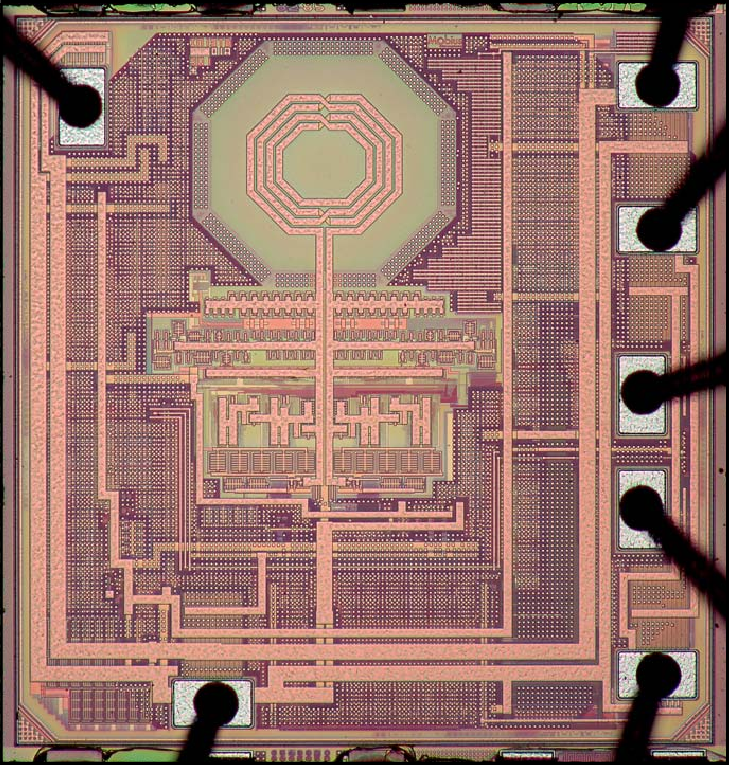
Of the basic electronic components, only the induction coil remains. It might seem that the construction of such elements in silicon is impossible. After all, a coil needs a core in order to operate, whether it be ferromagnetic or simply air, that is, in fact, there will be none, so the construction of such a structure on a silicon substrate seems impossible. But nothing could be further from the truth, silicon coils do exist, although they are used extremely rarely.
Induction coils in silicon are built similar to those hidden in payment cards every day. A metal coil of specific dimensions is placed on a flat substrate so that the specific electrical parameters of the element are achieved. You can see an example of such a coil in the photo above. Although the construction of an inductive coil is possible, designers avoid this type of structure. The reason, as in the case of previous elements, is their low quality and difficulty in obtaining the desired properties. Besides, as you can see in the photo, the coil in silicon occupies a huge area, which is always too little anyway.
Thus, we learned about the construction of integrated circuits, types of doping and basic silicon electronic components. As it turns out, these structures are not ideal elements, and on the contrary, they are quite problematic, but it is important to remember that integrated circuits primarily use transistors, which I will tell you about in the next material, the link to which, you will find below.
In today's dynamic world of electronics, we are constantly using advanced technologies that enable us to perform tasks faster, more efficiently and more conveniently. One of the most remarkable developments that has affected our daily reality is the invention of the integrated circuit. These small but powerful electronic components, typically containing hundreds, thousands or even millions of elements on a single silicon wafer. Chips have revolutionized our world in ways we could not even imagine before. But in order to explore the history of integrated circuits, we need to go all the way back to the 1920s, to the days of tube designs.
Any electronic equipment must be powered in some way, without the right voltage it will not work at all or will work, but only for a fraction of a second. There are quite a few solutions and designs whose task is to bring energy to the designed circuit. Some of the most commonly used are linear stabilizers and voltage converters. We will leave stabilizers for another material, while today I would like to tell you a little about the operation and design of inverters. In addition, we will also look at their problems and try to solve them.
Sources:
- https://electronics.stackexchange.com/questions/573412/which-technique-is-used-to-create-high-value-resistance-inside-a-ic
- https://www.britannica.com/technology/transistor/Silicon-transistors
- https://learn.sparkfun.com/tutorials/integrated-circuits/all
- https://www.sparkfun.com/news/384?_gl=1*7jsbvm*_ga*Mjc2ODExMTI0LjE2OTIxMTQ3NDA.*_ga_T369JS7J9N*MTY5MjExNDczOS4xLjAuMTY5MjExNDczOS42MC4wLjA.&_ga=2.42616677.1781712633.1692114740-276811124.1692114740
- https://www.idc-online.com/technical_references/pdfs/electronic_engineering/Integrated_Resistors.pdf
- https://electronics.stackexchange.com/questions/573412/which-technique-is-used-to-create-high-value-resistance-inside-a-ic
- https://anysilicon.com/ic-design/
- https://passive-components.eu/silicon-as-a-capacitor-dielectric-strengths-limitations/
- https://miscircuitos.com/an-overview-of-on-chip-inductors-for-integrated-circuits-ic-types-pro-cons/
- https://www.researchgate.net/publication/224169588_A_Silicon_Die_as_a_Frequency_Source
